表紙
|
|
|
- かんじ なかじゅく
- 5 years ago
- Views:
Transcription
1
2

3 Akira Fujishima 2005.Vo.3 1


4 Kiyoshi kanamura Vol.3
5 Rechargeable Lithium Ion-Battery Active Material Liquid Electrolyte σ = S cm -1 3D Interface of Solid / Liquid Binding Material 2005.Vol.3 3
 Ti(OCH(CH 3 ) 2 ) 4 (1) H 2 O")
 Li-La-Ti-O Sol 4 2005.Vol.")
6 (CH 3 ) 2 CHOH (20) (Molar Ratio) CH 3 COOH (10) Ti(OCH(CH 3 ) 2 ) 4 (1) H 2 O (140) CH 3 COOLi (0.35) La(CH 3 COO) H 2 O (0.55) Li-La-Ti-O Sol Vol.3

7 2005.Vol.3 5

8 Vol.3

9 2005.Vol.3 7

10 Vol.3
11 Three-dimensionally ordered macroporous (3DOM) silica silica membrane Polymer Electrolyte H + Porosity 74% Matrix Polymer expansion is mechanically suppressed by porous silica matrix. Proton conductor (liquid, polymer) Ordered macroporous silica matrix Low methanol cross-over High proton conductivity 2005.Vol.3 9

12 Vol.3
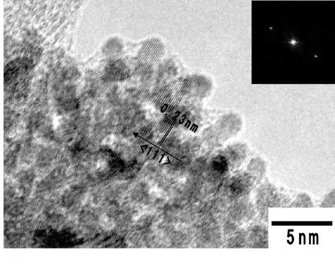
![Current Density [ma/cm 2 ] 60 50 40 30 20 10 0 After polymerization](/docs-images/91/105129756/images/13-0.jpg "Before polymerization 0 0.2 0.4 0.6 0.8 Potential [V vs. Ag/AgCl] 2005.")
13 Current Density [ma/cm 2 ] After polymerization Before polymerization Potential [V vs. Ag/AgCl] 2005.Vol.3 11
14 Vol.3


15 Tsuyoshi Kijima Vol.3 13

16 AFM Vol.3


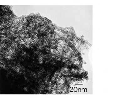
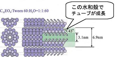
17 SBH Tween Vol.3 15
18 0.5M H2SO4 SBH SBH/Pt 10 SBH Vol.3

 AFM Tween60 Tween60 HOPG")
19 0.5M H2SO4 SBH 0.6V 0.75V Johnson Matthey HiSPEC 4000 に 1g SBH/Pt 10 AFM Tween60 (HOPG) AFM Tween60 Tween60 HOPG 2005.Vol.3 17
 RF")
 80")

20 OH R F (CTAB) RF NaOH RF /CTA 250 (TMB) 80 2 (H + ) RF Vol.3

21 ( ) 2005.Vol.3 19
22 Vol.3

23 Akihiko Kudo 2005.Vol.3 21

24 Vol.3

25 2005.Vol.3 23

26 Vol.3
27 m 2005.Vol.3 25

28 Vol.3

29 2005.Vol.3 27

30 Vol.3
31 2005.Vol.3 29
32 Vol.3


33 Hideomi Koinuma Vol.3 31

34 Vol.3

35 2005.Vol.3 33

36 Vol.3

37 2005.Vol.3 35
38 Vol.3

39 2005.Vol.3 37
40 1. H. Koinuma & I. Takeuchi. "Combinatorial solid-state chemistry of inorganic materials". Nature Materials 3, 429 (2004). 2. A. Tsukazaki et al. "Repeated temperature modulation epitaxy for p-type doping and light-emitting diode based on ZnO". Nature Materials 4, 42 (2005). 3. Y. Matsumoto et al. "Room-temperature ferromagnetism in transparent transition metal-doped titanium dioxide". Science 291, 854 (2001). 4. Y. Yamamoto et al. "Homo-epitaxial growth of rutile TiO2 film on step and terrace structured substrate". Appl. Surf. Sci. 238, 189 (2004). 5. T. Koida et al. "Temperature-gradient epitaxy under in situ growth mode diagnostics by scanning reflection high-energy electron diffraction". Appl. Phys. Lett. 80, 565 (2002). 6. M. Sumiya et al. "SIMS analysis of ZnO films co-doped with N and Ga by temperature gradient pulsed laser deposition". Appl. Surf. Sci. 223, 206 (2004). 7. M. Sumiya & S. Fuke. "Effect of treatments of sapphire substrate on growth of GaN film". Appl. Surf. Sci. 244, 269 (2005). 8. K. Itaka et al. "Combinatorial approach to the fabrication of organic thin films". Appl. Surf. Sci. 252, 2562 (2006). 9. J. Yamaguchi et al. "An in-situ Fabrication and Characterization System Developed for High Performance Organic Semiconductor Devices". Jpn. J. Appl. Phys. 44, 3757 (2005). 10. K. Arai et al. "Fabrication of liquid crystal polymer films and their passivation effect for organic devices". Jpn. J. Appl. Phys. 44, 4164 (2005). 11. T. Edura et al. "Electrical characterization of single grain and single grain boundary of pentacene thin film by nano-scale electrode array". Curr. Appl. Phys. 6, 109 (2006) Vol.3

41 Kunihito Koumoto Vol.3 39

42 Vol.3

43 2005.Vol.3 41

44 Vol.3

45 m m 2005.Vol.3 43


46 Vol.3
47 2005.Vol.3 45


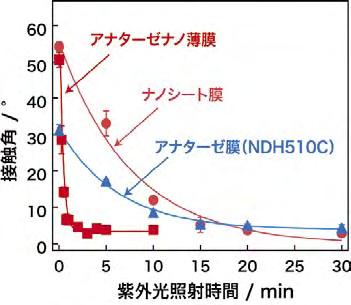
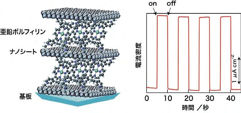
48 Takayoshi Sasaki Vol.3

49 0.5H 2005.Vol.3 47

50 Bednorz Müller Vol.3

51 2005.Vol.3 49
52 Vol.3

53 2005.Vol.3 51

54 Vol.3

55 2005.Vol.3 53

56 Vol.3


57 Yoshihiro NakatoSasaki Vol.3 55

58 μ current density / ma cm -2 voltage[v] Vol.3

59 2005.Vol.3 57


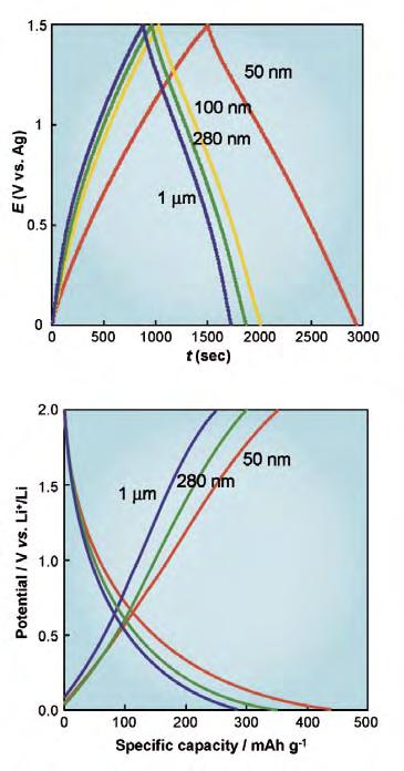
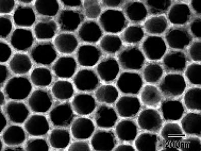
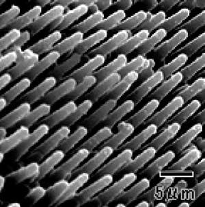
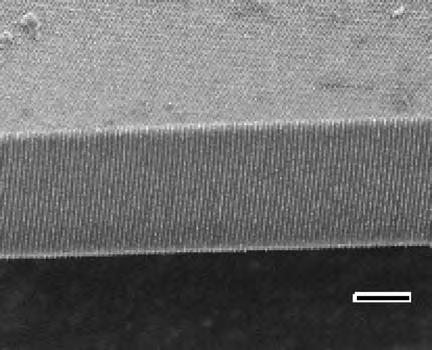
60 Vol.3

61 2005.Vol.3 59
62 Vol.3

63 μ μ μ 2005.Vol.3 61

64 Vol.3

65 Kaname Matsumoto Vol.3 63
66 B=μ Vol.3
67 - α /2 ξ 2005.Vol.3 65


68 d ( θ ) を比較したものである θ = 90 (B//c) に現れる鋭い J Vol.3
![ε ( θ )=[cos θ + γ θ ] ( θ )=B (0)/](/docs-images/91/105129756/images/69-1.jpg "ε ( θ ) と表わされる ( θ ) d 2005.Vol.")
69 ε ( θ )=[cos θ + γ θ ] ( θ )=B (0)/ ε ( θ ) と表わされる ( θ ) d 2005.Vol.3 67

70 d Vol.3
71 d μ m 厚程度作製することで得られる これらの SmBCO 膜は 350 酸素気流中でアニール処理を施した d 2005.Vol.3 69
72 d μ m 厚 μ m Vol.3


73 Junichi Yamaki Vol.3 71

74 Vol.3
75 2005.Vol.3 73

76 Vol.3

77 2005.Vol.3 75

78 Vol.3

79 2005.Vol.3 77

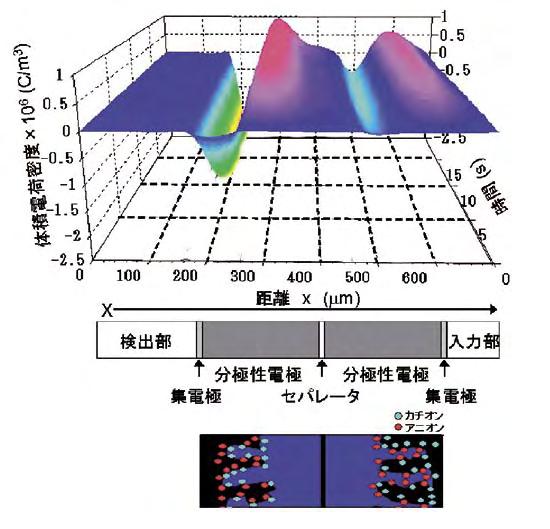
80 Tamio Ikeshoj Vol.3
81 2005.Vol.3 79
82 Vol.3

83 2005.Vol.3 81
 45 82 2005.")
84 K. Okazaki et al., Appl. Catal. A (2005) Vol.3


85 Pt10/Graphen The Pt-H bond length 1st 2nd 3rd 3.02Å 3.26Å 3.30Å Valence electron density distribution 2005.Vol.3 83
86 [2] M. Otani and O. Sugino, to be published in Phys. Rev. B (2006) Gröthuss Gröthuss Vol.3

87 2005.Vol.3 85
88
89
90
スライド 1
 Matsuura Laboratory SiC SiC 13 2004 10 21 22 H-SiC ( C-SiC HOY Matsuura Laboratory n E C E D ( E F E T Matsuura Laboratory Matsuura Laboratory DLTS Osaka Electro-Communication University Unoped n 3C-SiC
研究成果報告書
 EL EL 17% 1.5 (F. Li, et al. Org. Elect., Vol. 8, 635, 2007 ) (S.Hore, et al., Sol. Energy Mater. Sol. Cells, pp. Vol. 90, 1176, 2006) (C. Haase et al., Proc. of SPIE, Vol. 6645, 66450W, 2007) (T. Fukuda
1
 4 Nano Device Technologies From New Functions of Extreme Substances to Telecommunication Technologies 4-1 Controlling Intermolecular Interactions using Nano- Structural Molecules OTOMO Akira, YOKOYAMA
untitled
 254nm UV TiO 2 20nm :Sr 5 Ta 4 O 15 3 4 KEY-1 KEY-2 (Ti,Nb,Ta) 5 KEY-1 KEY-2 6 7 NiO/ Sr 2 Ta 2 O 7 mmol h -1 g -1 20 15 10 5 H 2 O 2 H 2 O 2 0 0 2 4 6 8 10 12 NiO/Sr 2 Ta 2 O 7 The synthesis of photocatalysts
SPring8菅野印刷.PDF
 20021219Spring-8 Ah/kg Ah/dm 3 Li -3.01 540 3860 2090 Na -2.71 970 1160 1140 Al -1.66 2690 2980 8100 Zn -0.76 7140 820 5800 Fe -0.44 7850 960 7500 Cd -0.40 8650 480 4100 Pb -0.13 11340 260 2900 H 2 0
42 3 u = (37) MeV/c 2 (3.4) [1] u amu m p m n [1] m H [2] m p = (4) MeV/c 2 = (13) u m n = (4) MeV/c 2 =
![42 3 u = (37) MeV/c 2 (3.4) [1] u amu m p m n [1] m H [2] m p = (4) MeV/c 2 = (13) u m n = (4) MeV/c 2 =](/thumbs/73/68712188.jpg "42 3 u = (37) MeV/c 2 (3.4) [1] u amu m p m n [1] m H [2] m p = (4) MeV/c 2 = (13) u m n = (4) MeV/c 2 =") 3 3.1 3.1.1 kg m s J = kg m 2 s 2 MeV MeV [1] 1MeV=1 6 ev = 1.62 176 462 (63) 1 13 J (3.1) [1] 1MeV/c 2 =1.782 661 731 (7) 1 3 kg (3.2) c =1 MeV (atomic mass unit) 12 C u = 1 12 M(12 C) (3.3) 41 42 3 u
3 3.1 3.1.1 kg m s J = kg m 2 s 2 MeV MeV [1] 1MeV=1 6 ev = 1.62 176 462 (63) 1 13 J (3.1) [1] 1MeV/c 2 =1.782 661 731 (7) 1 3 kg (3.2) c =1 MeV (atomic mass unit) 12 C u = 1 12 M(12 C) (3.3) 41 42 3 u
研究成果報告書(基金分)
") (DMS) 1 3 DMS 2 4 DMS II-VI CdTe ZnTe 2 4 DMS 2 4 DMS II-VI 2 3d 4 3d (MBE) II-VI ZnTe CdTe 3d Mn, Cr, Fe 2 4 DMS MBE X (XRD)X (XAFS) II (SQUID) (a) 4 DMS (Cd,Mn,Cr)Te 4 DMS II-VI CdTe 2 Mn, Cr (Cd,Mn,Cr)Te
(DMS) 1 3 DMS 2 4 DMS II-VI CdTe ZnTe 2 4 DMS 2 4 DMS II-VI 2 3d 4 3d (MBE) II-VI ZnTe CdTe 3d Mn, Cr, Fe 2 4 DMS MBE X (XRD)X (XAFS) II (SQUID) (a) 4 DMS (Cd,Mn,Cr)Te 4 DMS II-VI CdTe 2 Mn, Cr (Cd,Mn,Cr)Te
研究室ガイダンス(H28)福山研.pdf
福山研.pdf") 1 2 3 4 5 4 He M. Roger et al., JLTP 112, 45 (1998) A.F. Andreev and I.M. Lifshitz, Sov. Phys. JETP 29, 1107 (1969) Born in 2004 (hcp 4 He) E. Kim and M.H.W. Chan, Nature 427, 225 (2004); Science 305,
1 2 3 4 5 4 He M. Roger et al., JLTP 112, 45 (1998) A.F. Andreev and I.M. Lifshitz, Sov. Phys. JETP 29, 1107 (1969) Born in 2004 (hcp 4 He) E. Kim and M.H.W. Chan, Nature 427, 225 (2004); Science 305,
From Evans Application Notes
 3 From Evans Application Notes http://www.eaglabs.com From Evans Application Notes http://www.eaglabs.com XPS AES ISS SSIMS ATR-IR 1-10keV µ 1 V() r = kx 2 = 2π µν x mm 1 2 µ= m + m 1 2 1 k ν = OSC 2
42 1 Fig. 2. Li 2 B 4 O 7 crystals with 3inches and 4inches in diameter. Fig. 4. Transmission curve of Li 2 B 4 O 7 crystal. Fig. 5. Refractive index
 MEMOIRS OF SHONAN INSTITUTE OF TECHNOLOGY Vol. 42, No. 1, 2008 Li 2 B 4 O 7 (LBO) *, ** * ** ** Optical Scatterer and Crystal Growth Technology of LBO Single Crystal For Development with Optical Application
16 (16) poly-si mJ/cm 2 ELA poly-si super cooled liquid, SCL [3] a-si poly-si [4] solid phase crystalization, SPC [5] mJ/cm 2 SPC SCL (di
![16 (16) poly-si mJ/cm 2 ELA poly-si super cooled liquid, SCL [3] a-si poly-si [4] solid phase crystalization, SPC [5] mJ/cm 2 SPC SCL (di](/thumbs/82/84964999.jpg "16 (16) poly-si mJ/cm 2 ELA poly-si super cooled liquid, SCL [3] a-si poly-si [4] solid phase crystalization, SPC [5] mJ/cm 2 SPC SCL (di") (15) 15 ELA により形成された poly-si 結晶成長様式 - グレイン形状と水素の関係 - Crystal Growth Mode of Poly-Si Prepared by ELA -Relationship between the Grain Morphology and ydrogens- Naoya KAWAMOTO (Dept. of Electrical and Electronic
(15) 15 ELA により形成された poly-si 結晶成長様式 - グレイン形状と水素の関係 - Crystal Growth Mode of Poly-Si Prepared by ELA -Relationship between the Grain Morphology and ydrogens- Naoya KAWAMOTO (Dept. of Electrical and Electronic
untitled
 2013 74 Tokyo Institute of Technology AlGaN/GaN C Annealing me Dependent Contact Resistance of C Electrodes on AlGaN/GaN, Tokyo Tech.FRC, Tokyo Tech. IGSSE, Toshiba, Y. Matsukawa, M. Okamoto, K. Kakushima,
卒 業 研 究 報 告
 16 2 17 ...1 1.1.1 1.2.3...4 2.1. 4 2.2. 4 2.3. 5 2.3.1.. 5 2.3.2. 10 2.3.3.. 11 2.4.....11 2.4.1 LCD.....12 2.4.2 EL.. 13 2.4.3. 14 2.4.4. 15 2.4.5 SAW... 15 2.4.6.. 16 2.5.....16 2.5.1 CVD.....16 2.5.2..
薄膜結晶成長の基礎3.dvi
 3 464-8602 1 [1] 2 3 (epitaxy) (homoepitaxy) (heteroepitaxy) 1 Makio Uwaha. E-mail:uwaha@nagoya-u.jp; http://slab.phys.nagoya-u.ac.jp/uwaha/ 2 3.1 [2] (strain) r u(r) ɛ αγ (r) = 1 ( uα + u ) γ (3.1) 2
chap1_MDpotentials.ppt
 simplest Morse : simplest (1 Well-chosen functional form is more useful than elaborate fitting strategies!! Phys. Rev. 34, 57 (1929 ( 2 E ij = D e 1" exp("#(r ij " r e 2 r ij = r i " r j r ij =r e E ij
SPring-8_seminar_
 X 21 SPring-8 XAFS 2016 (= ) X PC cluster Synchrotron TEM-EELS XAFS / EELS HΨ k = E k Ψ k XANES/ELNES DFT ( + ) () WIEN2k, Elk, OLCAO () CASTEP, QUANTUM ESPRESSO FEFF, GNXAS, etc. Bethe-Salpeter (BSE)
1 9 v.0.1 c (2016/10/07) Minoru Suzuki T µ 1 (7.108) f(e ) = 1 e β(e µ) 1 E 1 f(e ) (Bose-Einstein distribution function) *1 (8.1) (9.1)
 Minoru Suzuki T µ 1 (7.108) f(e ) = 1 e β(e µ) 1 E 1 f(e ) (Bose-Einstein distribution function) *1 (8.1) (9.1)") 1 9 v..1 c (216/1/7) Minoru Suzuki 1 1 9.1 9.1.1 T µ 1 (7.18) f(e ) = 1 e β(e µ) 1 E 1 f(e ) (Bose-Einstein distribution function) *1 (8.1) (9.1) E E µ = E f(e ) E µ (9.1) µ (9.2) µ 1 e β(e µ) 1 f(e )
1 9 v..1 c (216/1/7) Minoru Suzuki 1 1 9.1 9.1.1 T µ 1 (7.18) f(e ) = 1 e β(e µ) 1 E 1 f(e ) (Bose-Einstein distribution function) *1 (8.1) (9.1) E E µ = E f(e ) E µ (9.1) µ (9.2) µ 1 e β(e µ) 1 f(e )
PowerPoint プレゼンテーション
 1 45nm 2 2004 2007 2010 90* 65 45 4 10 25 * 100 10001 H16 45 2001-2003 2004-2007 65 45 MIRAI 3 Cu n+ n+ p+ p+ p n nmos pmos ITRS 2004 2007 2010 2013 2016 3.5 k 3.0 2.5 2.0 ITRS2001 ITRS2003 Low-k 1.5 1.0
untitled
 Tokyo Institute of Technology high-k/ In.53 Ga.47 As MOS - Defect Analysis of high-k/in.53 G a.47 As MOS Capacitor using capacitance voltage method,,, Darius Zade,,, Parhat Ahmet,,,,,, ~InGaAs high-k ~
< F836F A815B934B8D87955C E706466>
 92897 92893 10,000 92894 10,600 92895 11,300 92896 11,900 92897 11,900 92898 15,200 2 92888 92873 4,200 92874 4,200 92875 7,000 92876 7,000 92877 7,000 92878 8,800 92879 8,800 92880 13,300 92881 8,800
untitled
 213 74 AlGaN/GaN Influence of metal material on capacitance for Schottky-gated AlGaN/GaN 1, 2, 1, 2, 2, 2, 2, 2, 2, 2, 1, 1 1 AlGaN/GaN デバイス ① GaNの優れた物性値 ② AlGaN/GaN HEMT構造 ワイドバンドギャップ半導体 (3.4eV) 絶縁破壊電界が大きい
薄膜結晶成長の基礎4.dvi
 4 464-8602 1 [1] 2 (STM: scanning tunneling microscope) (AFM: atomic force microscope) 1 ( ) 4 LPE(liquid phase epitaxy) 4.1 - - - - (Burton Cabrera Frank) BCF [2] P f = (4.1) 2πmkB T 1 Makio Uwaha. E-mail:uwaha@nagoya-u.jp;
J. Mass Spectrom. Soc. Jpn.: 58(5), (2010)
, (2010)") J. Mass Spectrom. Soc. Jpn. Vol. 58, No. 5, 2010 REVIEW 9 Secondary Ion Mass Spectrometry (SIMS) SIMS SIMS Fundamentals of Mass Spectrometry Secondary Ion Mass Spectrometry (SIMS), Cluster SIMS, and Electrospray
J. Mass Spectrom. Soc. Jpn. Vol. 58, No. 5, 2010 REVIEW 9 Secondary Ion Mass Spectrometry (SIMS) SIMS SIMS Fundamentals of Mass Spectrometry Secondary Ion Mass Spectrometry (SIMS), Cluster SIMS, and Electrospray
èCò_ï\éÜ.pdf
 [Co/Ru] 20 Antiferromagnetic Exchange Coupling Energy in [Co/Ru] 20 19 1...1 1.1...1 1.2...1 1.2.1...1 1.2.2...2 1.3...2 1.4...3 1.4.1...3 1.4.2...5 1.5...5 1.5.1...5 1.5.2 SF...6 1.5.3 TAMR...6 2...8
Temperature Rise in a Birefringent Substrate by RF Discharge Plasma Koichi Takaki, Member, Kunioh Sayama, Student Member, Atsushi Takahashi, Student M
 Temperature Rise in a Birefringent Substrate by RF Discharge Plasma Koichi Takaki, Member, Kunioh Sayama, Student Member, Atsushi Takahashi, Student Member, Tamiya Fujiwara, Member (Iwate University),
untitled
 1 / 37 5-4 6.1 1 2 / 37 1 (1) FePt AuAg (2) CdSe ZnSXY 2 O 3 X X : ZnO (3) SiO 2 (4) (5) 2 1 3 / 37 1 (1) FePt AuAg (2) CdSe ZnSXY 2 O 3 X X : ZnO (3) SiO 2 (4) (5) 3 4 / 37 1Tbits/cm 2 HD FePt FePt 110nm
Microsoft PowerPoint - 14.菅谷修正.pptx
 InGaAs/系量子ドット太陽電池の作製 革新デバイスチーム 菅谷武芳 電子 バンド3:伝導帯 E3 E3 E 正孔 バンド:中間バンド 量子ドット超格子 ミニバンド 量子ドットの井戸型 ポテンシャル バンド:価電子帯 量子ドット太陽電池のバンド図 6%を超える理想的な量子ドット太陽 電池実現には E3として1 9eVが必要 量子ドット超格子太陽電池 理論上 変換効率6%以上 集光 を採用 MBE
支援財団研究活動助成 生体超分子を利用利用した 3 次元メモリデバイスメモリデバイスの研究 奈良先端科学技術大学院大学物質創成科学研究科小原孝介
 2009.3.10 支援財団研究活動助成 生体超分子を利用利用した 3 次元メモリデバイスメモリデバイスの研究 奈良先端科学技術大学院大学物質創成科学研究科小原孝介 研究背景研究背景研究背景研究背景データデータデータデータの種類種類種類種類データデータデータデータの保存保存保存保存パソコンパソコンパソコンパソコンパソコンパソコンパソコンパソコンデータデータデータデータデータデータデータデータ音楽音楽音楽音楽音楽音楽音楽音楽写真写真写真写真記録媒体記録媒体記録媒体記録媒体フラッシュメモリフラッシュメモリフラッシュメモリフラッシュメモリ動画動画動画動画
TOP10 Innovations A triple-junction compound solar module with a conversion efficiency of 31.17%. Source SHARP CORPORATION (
 A triple-junction compound solar module with a conversion efficiency of 31.17%. Source SHARP CORPORATION (http://www.sharp.co.jp/corporate/news/160519-a.html) 2017 Zentrum für Sonnenenergie- und Wasserstoff-Forschung
 1-x x µ (+) +z µ ( ) Co 2p 3d µ = µ (+) µ ( ) W. Grange et al., PRB 58, 6298 (1998). 1.0 0.5 0.0 2 1 XMCD 0-1 -2-3x10⁻³ 7.1 7.2 7.7 7.8 8.3 8.4 up E down ρ + (E) ρ (E) H, M µ f + f E F f + f f + f X L
Vol. 21, No. 2 (2014) W 3 mm SUS304 Ni 650 HV 810 HV Ni Ni Table1 Ni Ni μm SUS mm w 50 mm l 3 mm t 2.2 Fig. 1 XY Fig. 3 Sch
 W 3 mm SUS304 Ni 650 HV 810 HV Ni Ni Table1 Ni Ni μm SUS mm w 50 mm l 3 mm t 2.2 Fig. 1 XY Fig. 3 Sch") 110 : 565-0871 2-1 567-0871 11-1 660-0811 1-9 - 1 tanigawa@jwri.osaka - u.ac.jp Influence of Laser Beam Profile on Cladding Layer TANIGAWA Daichi, ABE Nobuyuki, TSUKAMOTO Masahiro, HAYASHI Yoshihiko, YAMAZAKI
110 : 565-0871 2-1 567-0871 11-1 660-0811 1-9 - 1 tanigawa@jwri.osaka - u.ac.jp Influence of Laser Beam Profile on Cladding Layer TANIGAWA Daichi, ABE Nobuyuki, TSUKAMOTO Masahiro, HAYASHI Yoshihiko, YAMAZAKI
** Department of Materials Science and Engineering, University of California, Los Angeles, CA 90025, USA) Preparation of Magnetopulmbite Type Ferrite
 Preparation of Magnetopulmbite Type Ferrite") ** Department of Materials Science and Engineering, University of California, Los Angeles, CA 90025, USA) Preparation of Magnetopulmbite Type Ferrite Thin Films by Dip-Coating Method and Magnetic Properties
** Department of Materials Science and Engineering, University of California, Los Angeles, CA 90025, USA) Preparation of Magnetopulmbite Type Ferrite Thin Films by Dip-Coating Method and Magnetic Properties
untitled
 27.2.9 TOF-SIMS SIMS TOF-SIMS SIMS Mass Spectrometer ABCDE + ABC+ DE + Primary Ions: 1 12 ions/cm 2 Molecular Fragmentation Region ABCDE ABCDE 1 15 atoms/cm 2 Molecular Desorption Region Why TOF-SIMS?
物理予稿01-
 http://www.riken.jp/lab/dri/newpro/ 1 7 11 00 11 30 8 11 30 12 00 10 12 00 12 30 12 12 30 12 40 12 40 13 40 15 13 40 14 15 16 14 15 14 20 19 14 20 14 40 20 14 40 15 00 22 15 00 15 20 24 15 20 15 40 26
 Influence of Material and Thickness of the Specimen to Stress Separation of an Infrared Stress Image Kenji MACHIDA The thickness dependency of the temperature image obtained by an infrared thermography
スライド 1
 Front End Processes FEP WG - - NEC 1 ITRS2006 update 2 ITRS vs. 2-1 FET 2-2 Source Drain Extension 2-3 Si-Silicide 2-4 2-5 1 , FEP Front End Processes Starting Materials: FEP Si,, SOI SOI: Si on Insulator,
X X 1. 1 X 2 X 195 3, 4 Ungár modified Williamson-Hall/Warren-Averbach 5-7 modified modified Rietveld Convolutional Multiple Whole Profile CMWP 8 CMWP
 X X a a b b c Characterization of dislocation evolution during work hardening of stainless steels by using XRD line-profile analysis Tomoaki KATO a, Shigeo SATO a, Yoichi SAITO b, Hidekazu TODOROKI b and
技術創造の社会的条件
 1999 10 21 21 i ... 1 1... 3 1-1. 20...3 1900 1945 3 1945 198x 4 198x 1999 5 1-2....7 1945 198x 7 HEMT 8 198x 1999 9 9 1-3....11 11 12 13 18 2 New Institutions... 21 2-1....21 22 24 26 2-2....27 28 29
Corrosion Wear of Alloy Tool Steel (SKD 11) Coated with VC and Precipitation Hardening Stainless Steel (SUS 630) in Sodium Chloride Aqueous Solution T
 Coated with VC and Precipitation Hardening Stainless Steel (SUS 630) in Sodium Chloride Aqueous Solution T") Corrosion Wear of Alloy Tool Steel (SKD 11) Coated with VC and Precipitation Hardening Stainless Steel (SUS 630) in Sodium Chloride Aqueous Solution Toshiyuki TANAKI*, Makoto YUASA** and Isao SEKINE***
Corrosion Wear of Alloy Tool Steel (SKD 11) Coated with VC and Precipitation Hardening Stainless Steel (SUS 630) in Sodium Chloride Aqueous Solution Toshiyuki TANAKI*, Makoto YUASA** and Isao SEKINE***
The Plasma Boundary of Magnetic Fusion Devices
 ASAKURA Nobuyuki, Japan Atomic Energy Research Institute, Naka, Ibaraki 311-0193, Japan e-mail: asakuran@fusion.naka.jaeri.go.jp The Plasma Boundary of Magnetic Fusion Devices Naka Fusion Research Establishment,
d > 2 α B(y) y (5.1) s 2 = c z = x d 1+α dx ln u 1 ] 2u ψ(u) c z y 1 d 2 + α c z y t y y t- s 2 2 s 2 > d > 2 T c y T c y = T t c = T c /T 1 (3.
![d > 2 α B(y) y (5.1) s 2 = c z = x d 1+α dx ln u 1 ] 2u ψ(u) c z y 1 d 2 + α c z y t y y t- s 2 2 s 2 > d > 2 T c y T c y = T t c = T c /T 1 (3.](/thumbs/92/109966568.jpg "d > 2 α B(y) y (5.1) s 2 = c z = x d 1+α dx ln u 1 ] 2u ψ(u) c z y 1 d 2 + α c z y t y y t- s 2 2 s 2 > d > 2 T c y T c y = T t c = T c /T 1 (3.") 5 S 2 tot = S 2 T (y, t) + S 2 (y) = const. Z 2 (4.22) σ 2 /4 y = y z y t = T/T 1 2 (3.9) (3.15) s 2 = A(y, t) B(y) (5.1) A(y, t) = x d 1+α dx ln u 1 ] 2u ψ(u), u = x(y + x 2 )/t s 2 T A 3T d S 2 tot S
5 S 2 tot = S 2 T (y, t) + S 2 (y) = const. Z 2 (4.22) σ 2 /4 y = y z y t = T/T 1 2 (3.9) (3.15) s 2 = A(y, t) B(y) (5.1) A(y, t) = x d 1+α dx ln u 1 ] 2u ψ(u), u = x(y + x 2 )/t s 2 T A 3T d S 2 tot S
Electrical contact characteristics of n-type diamond with Ti, Ni, NiSi2, and Ni3P electrodes
 Electrical contact characteristics of n-type diamond with Ti, Ni, NiSi 2, and Ni 3 P electrodes 杉井 岩井研究室 12M36240 武正敦 1 注目を集めるワイドギャップ半導体 パワーエレクトロニクス ( 半導体の電力変換分野への応用 ) に期待 ワイドギャップ半導体に注目 Properties (relative
E 1/2 3/ () +3/2 +3/ () +1/2 +1/ / E [1] B (3.2) F E 4.1 y x E = (E x,, ) j y 4.1 E int = (, E y, ) j y = (Hall ef
![E 1/2 3/ () +3/2 +3/ () +1/2 +1/ / E [1] B (3.2) F E 4.1 y x E = (E x,, ) j y 4.1 E int = (, E y, ) j y = (Hall ef](/thumbs/81/83176619.jpg "E 1/2 3/ () +3/2 +3/ () +1/2 +1/ / E [1] B (3.2) F E 4.1 y x E = (E x,, ) j y 4.1 E int = (, E y, ) j y = (Hall ef") 4 213 5 8 4.1.1 () f A exp( E/k B ) f E = A [ k B exp E ] = f k B k B = f (2 E /3n). 1 k B /2 σ = e 2 τ(e)d(e) 2E 3nf 3m 2 E de = ne2 τ E m (4.1) E E τ E = τe E = / τ(e)e 3/2 f de E 3/2 f de (4.2) f (3.2)
4 213 5 8 4.1.1 () f A exp( E/k B ) f E = A [ k B exp E ] = f k B k B = f (2 E /3n). 1 k B /2 σ = e 2 τ(e)d(e) 2E 3nf 3m 2 E de = ne2 τ E m (4.1) E E τ E = τe E = / τ(e)e 3/2 f de E 3/2 f de (4.2) f (3.2)
研究成果報告書
 10m 2m Ge Si BaF2 ZnSZnSe Sb-Ge-Sn-S IIR-SF1 1 2 Tungsten SilicideWSi WSi () IIR-SF 1 Sb-Ge-Sn-S 0.85~11μm2.710μm 253 C Al Al 220μm He-Cd laser 1 Exposure Photoresist WSi (a) 500 nm Development RIE WSi
Undulator.dvi
 X X 1 1 2 Free Electron Laser: FEL 2.1 2 2 3 SACLA 4 SACLA [1]-[6] [7] 1: S N λ [9] XFEL OHO 13 X [8] 2 2.1 2(a) (c) z y y (a) S N 90 λ u 4 [10, 11] Halbach (b) 2: (a) (b) (c) (c) 1 2 [11] B y = n=1 B
untitled
 /Si FET /Si FET Improvement of tunnel FET performance using narrow bandgap semiconductor silicide Improvement /Si hetero-structure of tunnel FET performance source electrode using narrow bandgap semiconductor
1).1-5) - 9 -
.1-5) - 9 -") - 8 - 1).1-5) - 9 - ε = ε xx 0 0 0 ε xx 0 0 0 ε xx (.1 ) z z 1 z ε = ε xx ε x y 0 - ε x y ε xx 0 0 0 ε zz (. ) 3 xy ) ε xx, ε zz» ε x y (.3 ) ε ij = ε ij ^ (.4 ) 6) xx, xy ε xx = ε xx + i ε xx ε xy = ε
- 8 - 1).1-5) - 9 - ε = ε xx 0 0 0 ε xx 0 0 0 ε xx (.1 ) z z 1 z ε = ε xx ε x y 0 - ε x y ε xx 0 0 0 ε zz (. ) 3 xy ) ε xx, ε zz» ε x y (.3 ) ε ij = ε ij ^ (.4 ) 6) xx, xy ε xx = ε xx + i ε xx ε xy = ε
pp * Yw; Mq 1. 1L 20 cc [1] Sonoluminescence: Light emission from acoustic cavitation bubble. Pak-Kon Choi (Departm
![pp * Yw; Mq 1. 1L 20 cc [1] Sonoluminescence: Light emission from acoustic cavitation bubble. Pak-Kon Choi (Departm](/thumbs/94/118261255.jpg "pp * Yw; Mq 1. 1L 20 cc [1] Sonoluminescence: Light emission from acoustic cavitation bubble. Pak-Kon Choi (Departm") 73 7 2017 pp. 447 454 447 * 43.25.Yw; 78.60.Mq 1. 1L 20 cc [1] Sonoluminescence: Light emission from acoustic cavitation bubble. Pak-Kon Choi (Department of Physics, Meiji University, Kawasaki, 214 8571)
73 7 2017 pp. 447 454 447 * 43.25.Yw; 78.60.Mq 1. 1L 20 cc [1] Sonoluminescence: Light emission from acoustic cavitation bubble. Pak-Kon Choi (Department of Physics, Meiji University, Kawasaki, 214 8571)
a b Chroma Graphein Chromatography
 a b Chroma Graphein Chromatography (Stationary Phase) (Mobile Phase) CHROMATOGRAPHY GAS SFC LIQUID GSC GLC Column Planar NP RP IEC SEC TLC Paper Normal Phase Reverse Phase GPC GFC Thin Layer Chromato.
δδ 1 2 δ δ δ δ μ H 2.1 C 2.5 N 3.0 O 3.5 Cl 3.0 S μ
 1961. (Received January 15, 2013) 1) 1. 2. ph 2) 3) 2) 2) 2001 4 6) 7) ph ph ph 1961 1962 1. 2 1 1 δδ 1 2 δ δ δ δ μ 1 1 1 1. H 2.1 C 2.5 N 3.0 O 3.5 Cl 3.0 S 2.5 1 1. μ 1 3. 1 2. 1963 1,4- δ δ 1 3 2 δ
untitled
 2008-11/13 12 4 12 5 401 501 702 401 501 A-1 9:00-10:30 B-1 9:15-10:30 C-1 9:00-10:30 A-5 9:00-10:30 B-5 9:15-10:30 A A-2 10:45-12:15 B-2 10:45-12:15 C-2 10:45-12:15 A-6 10:45-12:15 B-6 10:45-12:15 A B
(Jackson model) Ziman) (fluidity) (viscosity) (Free v
 Ziman) (fluidity) (viscosity) (Free v") 1) 16 6 10 1) e-mail: nishitani@ksc.kwansei.ac.jp 0. 1 2 0. 1. 1 2 0. 1. 2 3 0. 1. 3 4 0. 1. 4 5 0. 1. 5 6 0. 1. 6 (Jackson model) 8 0. 1. 7 10. 1 10 0. 1 0. 1. 1 Ziman) (fluidity) (viscosity) (Free volume)(
1) 16 6 10 1) e-mail: nishitani@ksc.kwansei.ac.jp 0. 1 2 0. 1. 1 2 0. 1. 2 3 0. 1. 3 4 0. 1. 4 5 0. 1. 5 6 0. 1. 6 (Jackson model) 8 0. 1. 7 10. 1 10 0. 1 0. 1. 1 Ziman) (fluidity) (viscosity) (Free volume)(
Microsoft PowerPoint - tft.ppt [互換モード]
![Microsoft PowerPoint - tft.ppt [互換モード]](/thumbs/96/129523894.jpg "Microsoft PowerPoint - tft.ppt [互換モード]") 薄膜トランジスター 九州大学大学院 システム情報科学研究科 服部励治 薄膜トランジスターとは? Thin Film Transistor: TFT ソース電極 ゲート電極 ドレイン電極ソース電極ゲートドレイン電極 n poly 電極 a:h n n ガラス基板 p 基板 TFT 共通点 電界効果型トランジスター nmosfet 相違点 誘電膜上に作成される スタガー型を取りうる 薄膜トランジスター
薄膜トランジスター 九州大学大学院 システム情報科学研究科 服部励治 薄膜トランジスターとは? Thin Film Transistor: TFT ソース電極 ゲート電極 ドレイン電極ソース電極ゲートドレイン電極 n poly 電極 a:h n n ガラス基板 p 基板 TFT 共通点 電界効果型トランジスター nmosfet 相違点 誘電膜上に作成される スタガー型を取りうる 薄膜トランジスター
X線分析の進歩36 別刷
 X X X-Ray Fluorescence Analysis on Environmental Standard Reference Materials with a Dry Battery X-Ray Generator Hideshi ISHII, Hiroya MIYAUCHI, Tadashi HIOKI and Jun KAWAI Copyright The Discussion Group
1 2 LDA Local Density Approximation 2 LDA 1 LDA LDA N N N H = N [ 2 j + V ion (r j ) ] + 1 e 2 2 r j r k j j k (3) V ion V ion (r) = I Z I e 2 r
![1 2 LDA Local Density Approximation 2 LDA 1 LDA LDA N N N H = N [ 2 j + V ion (r j ) ] + 1 e 2 2 r j r k j j k (3) V ion V ion (r) = I Z I e 2 r](/thumbs/91/104998910.jpg "1 2 LDA Local Density Approximation 2 LDA 1 LDA LDA N N N H = N [ 2 j + V ion (r j ) ] + 1 e 2 2 r j r k j j k (3) V ion V ion (r) = I Z I e 2 r") 11 March 2005 1 [ { } ] 3 1/3 2 + V ion (r) + V H (r) 3α 4π ρ σ(r) ϕ iσ (r) = ε iσ ϕ iσ (r) (1) KS Kohn-Sham [ 2 + V ion (r) + V H (r) + V σ xc(r) ] ϕ iσ (r) = ε iσ ϕ iσ (r) (2) 1 2 1 2 2 1 1 2 LDA Local
11 March 2005 1 [ { } ] 3 1/3 2 + V ion (r) + V H (r) 3α 4π ρ σ(r) ϕ iσ (r) = ε iσ ϕ iσ (r) (1) KS Kohn-Sham [ 2 + V ion (r) + V H (r) + V σ xc(r) ] ϕ iσ (r) = ε iσ ϕ iσ (r) (2) 1 2 1 2 2 1 1 2 LDA Local
平成19年度
 1 2 3 4 H 3 H CC N + 3 O H 3 C O CO CH 3 CH O CO O CH2 CH 3 P O O 5 H H H CHOH H H H N + CHOH CHOH N + CH CH COO- CHOH CH CHOH 6 1) 7 2 ) 8 3 ) 4 ) 9 10 11 12 13 14 15 16 17 18 19 20 A A 0 21 ) exp( )
Mott散乱によるParity対称性の破れを検証
 Mott Parity P2 Mott target Mott Parity Parity Γ = 1 0 0 0 0 1 0 0 0 0 1 0 0 0 0 1 t P P ),,, ( 3 2 1 0 1 γ γ γ γ γ γ ν ν µ µ = = Γ 1 : : : Γ P P P P x x P ν ν µ µ vector axial vector ν ν µ µ γ γ Γ ν γ
 hν 688 358 979 309 308.123 Hz α α α α α α No.37 に示す Ti Sa レーザーで実現 術移転も成功し 図 9 に示すよ うに 2 時間は連続測定が可能な システムを実現した Advanced S o l i d S t a t e L a s e r s 2016, JTu2A.26 1-3. 今後は光周波 数比計測装置としてさらに改良 を加えていくとともに

薄膜結晶成長の基礎2.dvi
 2 464-8602 1 2 2 2 N ΔμN ( N 2/3 ) N - (seed) (nucleation) 1.4 2 2.1 1 Makio Uwaha. E-mail:uwaha@nagoya-u.jp; http://slab.phys.nagoya-u.ac.jp/uwaha/ 2 [1] [2] [3](e) 3 2.1: [1] 2.1 ( ) 1 (cluster) ( N


 Table-1 Formulation for testing water-based sunscreen gel containing P-ZnO. q. s.: quantum sufficit. J. Soc. Cosmet. Chem. Jpn. Vol. 42, No. 2 2008 103 Fig.-1 X-ray diffraction patterns of P-ZnO. Fig.
XFEL/SPring-8
 DEVELOPMENT STATUS OF RF SYSTEM OF INJECTOR SECTION FOR XFEL/SPRING-8 Takao Asaka 1,A), Takahiro Inagaki B), Hiroyasu Ego A), Toshiaki Kobayashi A), Kazuaki Togawa B), Shinsuke Suzuki A), Yuji Otake B),
6 2 T γ T B (6.4) (6.1) [( d nm + 3 ] 2 nt B )a 3 + nt B da 3 = 0 (6.9) na 3 = T B V 3/2 = T B V γ 1 = const. or T B a 2 = const. (6.10) H 2 = 8π kc2
![6 2 T γ T B (6.4) (6.1) [( d nm + 3 ] 2 nt B )a 3 + nt B da 3 = 0 (6.9) na 3 = T B V 3/2 = T B V γ 1 = const. or T B a 2 = const. (6.10) H 2 = 8π kc2](/thumbs/92/109118076.jpg "6 2 T γ T B (6.4) (6.1) [( d nm + 3 ] 2 nt B )a 3 + nt B da 3 = 0 (6.9) na 3 = T B V 3/2 = T B V γ 1 = const. or T B a 2 = const. (6.10) H 2 = 8π kc2") 1 6 6.1 (??) (P = ρ rad /3) ρ rad T 4 d(ρv ) + PdV = 0 (6.1) dρ rad ρ rad + 4 da a = 0 (6.2) dt T + da a = 0 T 1 a (6.3) ( ) n ρ m = n (m + 12 ) m v2 = n (m + 32 ) T, P = nt (6.4) (6.1) d [(nm + 32 ] )a
1 6 6.1 (??) (P = ρ rad /3) ρ rad T 4 d(ρv ) + PdV = 0 (6.1) dρ rad ρ rad + 4 da a = 0 (6.2) dt T + da a = 0 T 1 a (6.3) ( ) n ρ m = n (m + 12 ) m v2 = n (m + 32 ) T, P = nt (6.4) (6.1) d [(nm + 32 ] )a
note4.dvi
 10 016 6 0 4 (quantum wire) 4.1 4.1.1.6.1, 4.1(a) V Q N dep ( ) 4.1(b) w σ E z (d) E z (d) = σ [ ( ) ( )] x w/ x+w/ π+arctan arctan πǫǫ 0 d d (4.1) à ƒq [ƒg w ó R w d V( x) QŽŸŒ³ džq x (a) (b) 4.1 (a)

PowerPoint プレゼンテーション
 Drain Voltage (mv) 4 2 0-2 -4 0.0 0.2 0.4 0.6 0.8 1.0 Gate Voltage (V) Vds [V] 0.2 0.1 0.0-0.1-0.2-10 -8-6 -4-2 0 Vgs [V] 10 1000 1000 1000 1000 (LSI) Fe Catalyst Fe Catalyst Carbon nanotube 1~2 nm
Terahertz Color Scanner Takeshi YASUI Terahertz THz spectroscopic imaging is an interesting new tool for nondestructive testing, security screening, b
 Terahertz Color Scanner Takeshi YASUI Terahertz THz spectroscopic imaging is an interesting new tool for nondestructive testing, security screening, biological imaging, and other applications because of
The Phase Behavior of Monooleoylglycerol-Water Systems Mivoshi Oil & Fat Co.. Ltd. Faculty of Science and Technology, Science University of Tokyo Inst
 The Phase Behavior of Monooleoylglycerol-Water Systems Mivoshi Oil & Fat Co.. Ltd. Faculty of Science and Technology, Science University of Tokyo Institute of Colloid and Interface Science, Science University
Fig.2 Optical-microscope image of the Y face-cross sec- tion of the bulk domain structure of a 0.4-mm-thick MgO-LiNbO3 crystal after chemical etching.
 Blue EGreen Solid State Lasers Using MgO-LiNbO3 Periodic Domain Inverted Bulk Crystal and Their Applications Koji KAMIYAMA, Yoji OKAZAKI, and Akinori HARADA Fuji Photo Film. Co., Ltd., Miyanodai Technology
d (i) (ii) 1 Georges[2] Maier [3] [1] ω = 0 1
![d (i) (ii) 1 Georges[2] Maier [3] [1] ω = 0 1](/thumbs/94/121850661.jpg "d (i) (ii) 1 Georges[2] Maier [3] [1] ω = 0 1") 16 5 19 10 d (i) (ii) 1 Georges[2] Maier [3] 2 10 1 [1] ω = 0 1 [4, 5] Dynamical Mean-Field Theory (DMFT) [2] DMFT I CPA [10] CPA CPA Σ(z) z CPA Σ(z) Σ(z) Σ(z) z - CPA Σ(z) DMFT Σ(z) CPA [6] 3 1960 [7]
16 5 19 10 d (i) (ii) 1 Georges[2] Maier [3] 2 10 1 [1] ω = 0 1 [4, 5] Dynamical Mean-Field Theory (DMFT) [2] DMFT I CPA [10] CPA CPA Σ(z) z CPA Σ(z) Σ(z) Σ(z) z - CPA Σ(z) DMFT Σ(z) CPA [6] 3 1960 [7]

PFニュース indd
 最近の研究から X線回折法による Si(111) 表面における Ag の超構造および薄膜結晶配向性の研究 高橋敏男 1 * 田尻寛男 1 隅谷和嗣 1 秋本晃一 2 1 東京大学物性研究所 2 名古屋大学大学院工学研究科 Structural studies on superstructures and thin films of Ag on Si(111) by X-ray diffraction
(extended state) L (2 L 1, O(1), d O(V), V = L d V V e 2 /h 1980 Klitzing
 L (2 L 1, O(1), d O(V), V = L d V V e 2 /h 1980 Klitzing") 1 2 2.1 [1] [2] 2.1 STM [3, 4, 5, 6] 2.1: 2 ( 3 [1] ) [7, 8] [9]( 2.2) 2 2 2.1.1 (extended state) L (2 L 1, O(1), d O(V), V = L d V V 2.1.2 1985 2 e 2 /h 1980 Klitzing 2.1. 3 [7, 8] 2.2 [10] [8] 2.2: (a)
1 2 2.1 [1] [2] 2.1 STM [3, 4, 5, 6] 2.1: 2 ( 3 [1] ) [7, 8] [9]( 2.2) 2 2 2.1.1 (extended state) L (2 L 1, O(1), d O(V), V = L d V V 2.1.2 1985 2 e 2 /h 1980 Klitzing 2.1. 3 [7, 8] 2.2 [10] [8] 2.2: (a)
Microsoft PowerPoint - S-17.ppt
 In situ XRD および XAFS を用いた燃料電池アノード触媒電極の劣化解析 日本電気 ( 株 ) 松本匡史 m-matsumoto@jv.jp.nec.com 直接型メタノール燃料電池の PtRu アノードにおいて Ru は触媒被毒の原因である CO の酸化を促進する役割を持ち 電池出力の向上に不可欠な要素である しかし 長時間運転時には Ru が溶出し 性能が劣化する Ru 溶出は 運転時の
 46 12 3 1 ATP ( ) ATP ~P 1~P hyd Gº 1 1 1950 ~P hyd Gº Hansia et al. Biophys Chem 119: 127, 2006 ~P hyd Gº 1? ATP hyd Gº ATP ATP ATP ~P ε ~P George [BBA 223: 1, 1970] ~P 2) hyd Gº 1. ph Mg 2+ 2. 1 2 2
研究成果報告書
 COE 8 4 月 13 3 17-19,20-22 -COO - NH4 + 7 Fig.1 た 2 プ Fig.1 =0.154mol/L =0.1ml/min = 0.665g=20 PET AA PET Fig.2 AA AA PET PET AA Fig.2 PET AA-graft PET (3.17%, 6.37%) Fig.3 Fig.4 14 RDSv/h=1.10*e (-0.055d)
Research Reports on Information Science and Electrical Engineering of Kyushu University Vol.11, No.1, March 2006 Numerical Analysis of Scattering Atom
 九州大学学術情報リポジトリ Kyushu University Institutional Repository レーザーアブレーション原子蛍光分光法における放出原子の挙動解析 中村, 大輔九州大学大学院システム情報科学府電子デバイス工学専攻 : 博士後期課程 肥後谷, 崇九州大学大学院システム情報科学府電子デバイス工学専攻 : 修士課程 三洋電機株式会社 高尾, 隆之九州大学大学院システム情報科学研究院電子デバイス工学部門
fma20.PDF
 PZT TSC Measurement for Degraded and Damaged PZT Thin Films Capacitors Prepared by Sputtering. FeRAM MFIS : XRD, TEM : XRF, EDS, EPMA, SIMS : SPM, NDM? DLTS DLTS (TSC) (TSC) fatigue,, ( ) (1) (2) J T TSC
")
資料2 次世代太陽電池における計測機器
 第 9 回 先 端 計 測 分 析 技 術 機 器 開 発 小 委 員 会 2010 年 11 月 24 日 次 世 代 太 陽 電 池 における 計 測 機 器 韓 礼 元 次 世 代 太 陽 電 池 センター 1 太 陽 電 池 の 分 類 太 陽 電 池 シリコン 化 合 物 単 結 晶 結 晶 系 多 結 晶 薄 膜 系 (アモルファス マイクロクリスタル 等 ) 単 結 晶 ( GaAs

01_辻
 20 EBSD 2008.11.28 scanning electron microscope: SEM EBSD electron back scattering diffraction [1-4] 10 EBSD anisotropy polycrystal orientation texture EBSD EBSD EBSD EBSD Table 1 EBSD Table 1-10 mmφ
着色斜め蒸着膜の光学的性質~無機偏光膜への応用
 Anisotropy in the Optical Absorption of Metal-insulator Obliquely Deposited Thin Films The Application for an Inorganic Polarizer Motofumi Suzuki, Yasunori Taga Abstract An attempt has been made to clarify
68 JAXA-RR r v m Ó e ε 0 E = - Ó/ r f f 0 f 1 f = f 0 + f 1 x k f 1 = f k e ikx Ó = Ó k e ikx Ó k 3
 67 1 Landau Damping and RF Current Drive Kazuya UEHARA* 1 Abstract The current drive due to the rf travelling wave has been available to sustain the plasma current of tokamaks aiming the stational operation.
Ni PLD GdBa 2 Cu 3 O 7 x 2 6
 Ni PLD GdBa 2 Cu 3 O 7 x 2 6 1 1 1.1.................................. 1 1.2................................ 2 1.2.1......................... 3 1.3 RE 1 Ba 2 Cu 3 O 7 x...................... 3 1.3.1...............................
Introduction to Microfabrication
 2005 Introduction to Microfabrication 1 1.1 Microfabrication disciplines Microfabrication technologies IC industry and related industries MEMS, solar cells, flat-panel displays, optelectronics In-plane
4_Laser.dvi
 1 1905 A.Einstein 1917 A.Einstein 1954 C.H.Townes MASER Microwave Amplification by Stimulated Emission of Radiation 23.9 GHz 1.26 cm 1960 T.H.Maiman LASER Light Amplification by Stimulated Emissin of Radiation
Optical Lenses CCD Camera Laser Sheet Wind Turbine with med Diffuser Pitot Tube PC Fig.1 Experimental facility. Transparent Diffuser Double Pulsed Nd:
 *1 *2 *3 PIV Measurement of Field of the Wind Turbine with a med Diffuser Kazuhiko TOSHIMITSU *4, Koutarou NISHIKAWA and Yuji OHYA *4 Department of Mechanical Engineering, Matsue National Collage of Technology,
03_委託テーマ発表資料(その2)(p.89-p.134).pdf
(p.89-p.134).pdf") 89 MEMS 2 / 5-0 0-20 90 3 Beyond-CMOS CNT CNT CNT NEC 4 NEDO (80 NEDO 2008.05 Nature Nanotechnology NEDO (8 22 CNT CNT NEDOPJ CNT NEDO M 3 5 Nature Nanotechnology 3, 289-294 (2008) 6 9 7 8 92 9 (!!! '!!!
89 MEMS 2 / 5-0 0-20 90 3 Beyond-CMOS CNT CNT CNT NEC 4 NEDO (80 NEDO 2008.05 Nature Nanotechnology NEDO (8 22 CNT CNT NEDOPJ CNT NEDO M 3 5 Nature Nanotechnology 3, 289-294 (2008) 6 9 7 8 92 9 (!!! '!!!
untitled
 20101221JST (SiC - Buried Gate Static Induction Transistor: SiC-BGSIT) SOURCE GATE N source layer p + n p + n p + n p+ n drift layer n + substrate DRAIN SiC-BGSIT (mωcm 2 ) 200 100 40 10 4 1 Si limit
2004/4/16 (Power Technology) O 2 ( ) (Information Technology) ( ) Gas (4H) GaN andgap (ev) Electron mobility (cm 2 /Vs)
 O 2 ( ) (Information Technology) ( ) Gas (4H) GaN andgap (ev) Electron mobility (cm 2 /Vs)") ontents semicon.kuee.kyoto-u.ac.jp P 5.47 ev 1.12 ev Ge 0.66 ev Sn 0.08 ev DVD LSI, 3.20 ev GaN 3.42 ev ZnO 2004/4/16 (Power Technology) O 2 ( ) (Information Technology) ( ) Gas (4H) GaN andgap (ev) 1.12
ontents semicon.kuee.kyoto-u.ac.jp P 5.47 ev 1.12 ev Ge 0.66 ev Sn 0.08 ev DVD LSI, 3.20 ev GaN 3.42 ev ZnO 2004/4/16 (Power Technology) O 2 ( ) (Information Technology) ( ) Gas (4H) GaN andgap (ev) 1.12
( ) ( ) 87 ( ) 3 ( 150mg/l) cm cm 50cm a 2.0kg 2.0kg
 ( ) 87 ( ) 3 ( 150mg/l) cm cm 50cm a 2.0kg 2.0kg") 8 12 8 16.2004 1 2 The Effect of Planting Time and Mulching on Chinese Cabbage which to be Harvested from January to February Hitoshi KIMURA,Makoto MIYAGI and Masahito SUZUKI Summary In the cultivation
8 12 8 16.2004 1 2 The Effect of Planting Time and Mulching on Chinese Cabbage which to be Harvested from January to February Hitoshi KIMURA,Makoto MIYAGI and Masahito SUZUKI Summary In the cultivation


19 σ = P/A o σ B Maximum tensile strength σ % 0.2% proof stress σ EL Elastic limit Work hardening coefficient failure necking σ PL Proportional
 19 σ = P/A o σ B Maximum tensile strength σ 0. 0.% 0.% proof stress σ EL Elastic limit Work hardening coefficient failure necking σ PL Proportional limit ε p = 0.% ε e = σ 0. /E plastic strain ε = ε e
E 1 GeV E 10 GeV 1 2, X X , GeV 10 GeV 1 GeV GeV π
 169 8555 3 4 1 e-mail: kataoka.jun@waseda.jp 606 8502 e-mail: totani@kuastro.kyoto-u.ac.jp 305 0801 1 1 e-mail: kunihito.ioka@kek.jp 50 5 X 1 10 10 2008 3 2,000 542 2012 9 5 2. 1 3 E 1 GeV E 10 GeV 1 2,
X線分析の進歩45
 Advances in X-Ray Chemical Analysis, Japan, 45 (2014) ISSN 0911-7806 NaCl Color Center in NaCl Takuya TSUJI, Hiroyuki IWASAKI and Jun KAWAI NaCl Color Center in NaCl Takuya TSUJI, Hiroyuki IWASAKI and