Introduction to Microfabrication
|
|
|
- ようた かせ
- 4 years ago
- Views:
Transcription
1 2005 Introduction to Microfabrication 1
2 1.1 Microfabrication disciplines Microfabrication technologies IC industry and related industries MEMS, solar cells, flat-panel displays, optelectronics In-plane dimension: ~1um (0.1~100um) Out of plane dimension: 10nm~1um (0.1nm~100um) 1947: Invention of transistor 1 2
3 3
4 MEMS 1 m 1mm 10 m 20 mm CNT R e ρul UL = = µ ν 4
5 MEMS MEMS Interdisciplinary technology -TAS (micro Total Analysis Systems 5
6 Microelectronics / Optelectronic devices GaAs (III-V LED GaN, ZnO 6
 (Shape memory alloy : SMA)")
7 Mechanical devices (~150GPa) Cantilever, Diaphragm structures Pressure sensors Resonators Gyroscopes Switches Micromachines : micro-sensors & actuators (Piezoelectric materials) (Shape memory alloy : SMA) Si 7
8 Nanotechnology electron-beam lithography: drawing and fabrication of nanometer-sized structure Atomic Force Microscopy (AFM): characterization and manipulation of atomic structure. Superlattices for optelectronics GaAs/ Al x Ga 1-x As nano-machines of biological cells (molecular motors) 8
9 1.2 Substrates Base materials for deposition and etching Very convenient for microfabrication: Si variety of sizes, shapes : ~300mm variety of resistivities: 1m~20k -cm stable insulator layer : SiO 2 smooth surface single crystal with various orientations cheap strong (but fragile) Other substrates quartz gallium arsenide (GaAs) sapphire, alumina (Al 2 O 3 ) glass metal 9
10 1.3 Materials crystalline structure Deposition process 1.4 Surface and Interface Structure multi-layered structure surface layer roughness reflectivity chemical stability interlayer: internal stress, adhesion 10
11 1.5 Process Microfabrication process 1. High temperature process Thermal oxidation dopant diffusion 2. Thin-film deposition 3. Patterning Photolithography» simple CMOS 6 steps; 0.18umCMOS 25 steps 4. Layer transfer and bonding microfluidic channel packaging of MEMS devices 11
12 MEMS MEMS (Frontend) (Backend) Frontend CVD Backend
13 Si substrate Al thin film Si photoresist Al thin film Si Si photo mask Si Al thin film Si photoresist Al thin film Si 13
14 1.5.1 Arrhenius behaviour rate Ea = z( T )exp kt Many microfabrication processes show Arrheniustype dependence Etching Oxidation CVD 14
15 Lateral dimensions Device structure : 0.1~100um wire bonding, bump Microfluidics : capillaries, reservoirs Vertical dimension Aspect ratio 2:1 1um MEMS 10um 15
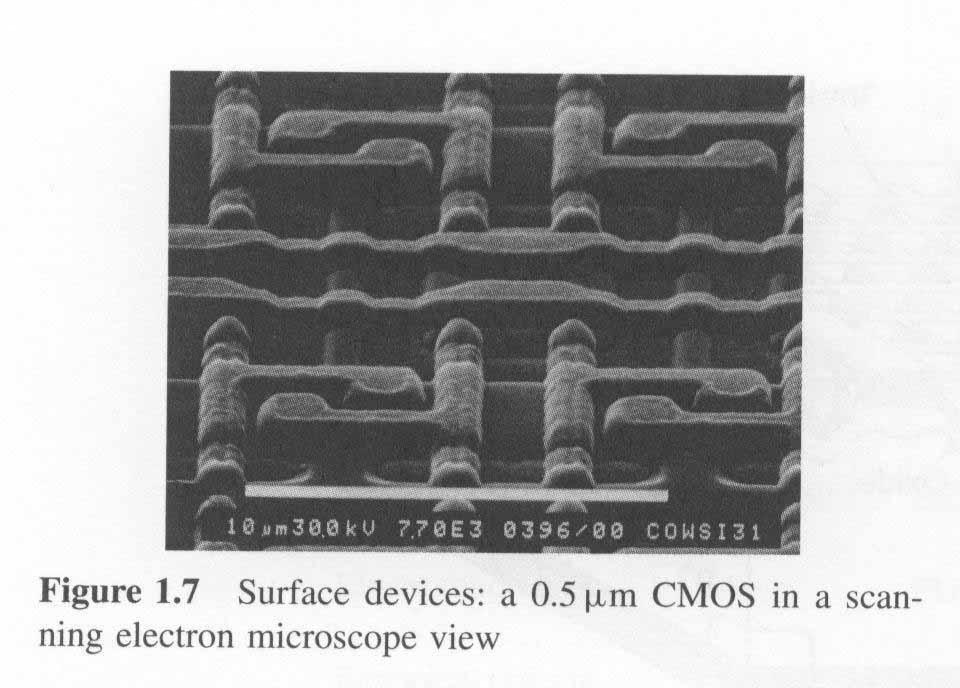
16 1.8 Devices Volume devices Currents are generated and transported through the wafer Device structures extend through the wafer Power transistor, thyristror, radiation detector, solar cell Surface devices Utilizing surface layer in the wafer IC, MOS, CCD» CMOS : only the top 5um layer is used 16
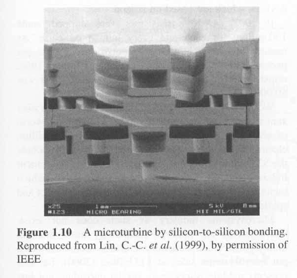
17 Thin-film devices Devices which are built by depositing and patterning thin films on wafers TFT (Thin Film Transistor) Surface micromechanical devices (switch, microfluidics) Membrane devices Devices on membrane structure Thermal isolation acoustic devices such as filter Stacked devices Devices which are made by layer transfer and bonding techniques vacuum cavity : pressure sensors, accelerometers, microfluidics : micropumps, microvalves, microchannels, 17
18 18

19 1.9 MOS transistor MOS : metal-oxide-semiconductor MOS 19
20 1.10 Cleanliness and yield 20
21 HEPA high efficiency particular air 1ft 3 (30cm 3 ) 0.5um 10 class100=log(100*(100/30) 3 )=M3.5 21
22 1.11Industries The electronics industry is based on Si semiconductor devices 2002: transistors were shipped, the cost was $10-7 a piece. 1968: 10 8 transistors, $1 a piece Device density : Moore s law 22
23 Moore s Law Gordon Moore: Former chairman of Intel IC 0.18 m Critical dimension (1/2) T/18 months DRAM (2) T/18 months 30nm 23
24 DRAM 24
03_委託テーマ発表資料(その2)(p.89-p.134).pdf
(p.89-p.134).pdf") 89 MEMS 2 / 5-0 0-20 90 3 Beyond-CMOS CNT CNT CNT NEC 4 NEDO (80 NEDO 2008.05 Nature Nanotechnology NEDO (8 22 CNT CNT NEDOPJ CNT NEDO M 3 5 Nature Nanotechnology 3, 289-294 (2008) 6 9 7 8 92 9 (!!! '!!!
89 MEMS 2 / 5-0 0-20 90 3 Beyond-CMOS CNT CNT CNT NEC 4 NEDO (80 NEDO 2008.05 Nature Nanotechnology NEDO (8 22 CNT CNT NEDOPJ CNT NEDO M 3 5 Nature Nanotechnology 3, 289-294 (2008) 6 9 7 8 92 9 (!!! '!!!
スライド 1
 Front End Processes FEP WG - - NEC 1 ITRS2006 update 2 ITRS vs. 2-1 FET 2-2 Source Drain Extension 2-3 Si-Silicide 2-4 2-5 1 , FEP Front End Processes Starting Materials: FEP Si,, SOI SOI: Si on Insulator,
16 (16) poly-si mJ/cm 2 ELA poly-si super cooled liquid, SCL [3] a-si poly-si [4] solid phase crystalization, SPC [5] mJ/cm 2 SPC SCL (di
![16 (16) poly-si mJ/cm 2 ELA poly-si super cooled liquid, SCL [3] a-si poly-si [4] solid phase crystalization, SPC [5] mJ/cm 2 SPC SCL (di](/thumbs/82/84964999.jpg "16 (16) poly-si mJ/cm 2 ELA poly-si super cooled liquid, SCL [3] a-si poly-si [4] solid phase crystalization, SPC [5] mJ/cm 2 SPC SCL (di") (15) 15 ELA により形成された poly-si 結晶成長様式 - グレイン形状と水素の関係 - Crystal Growth Mode of Poly-Si Prepared by ELA -Relationship between the Grain Morphology and ydrogens- Naoya KAWAMOTO (Dept. of Electrical and Electronic
(15) 15 ELA により形成された poly-si 結晶成長様式 - グレイン形状と水素の関係 - Crystal Growth Mode of Poly-Si Prepared by ELA -Relationship between the Grain Morphology and ydrogens- Naoya KAWAMOTO (Dept. of Electrical and Electronic
Microsoft PowerPoint - TMTinst_ _summerschool_akiyama
 1 2 3 4 5 6 7 8 9 10 590nm 2200nm 0 1.739 1.713 5 1.708 1.682 10 1.678 1.652 0-10 0.061061 0.061061 11 12 13 14 15 16 17 18 19 20 21 22 23 24 25 26 27 28 29 1.0 x1.0 0.5 x0.5 0.2 x0.2 0.1 x0.1 bg/30ms
untitled
 213 74 AlGaN/GaN Influence of metal material on capacitance for Schottky-gated AlGaN/GaN 1, 2, 1, 2, 2, 2, 2, 2, 2, 2, 1, 1 1 AlGaN/GaN デバイス ① GaNの優れた物性値 ② AlGaN/GaN HEMT構造 ワイドバンドギャップ半導体 (3.4eV) 絶縁破壊電界が大きい
untitled
 1 1-1 p-i-n 1-1 (CIS/CIGS CdTe ) (GaAs) (,,) (, ) (,,) Si Si Si (CIS/CIGS CdTe ) (GaAs) (,,) (, ) (,,) Si Si Si Si 1-2 HITHeterojunction with Intrinsic Thin layer 30 HIT 22.3NIKKEI MICRODEVICES, May,82-86(2008)
燃焼圧センサ
 49 Combustion Pressure Sensor Kouji Tsukada, Masaharu Takeuchi, Sanae Tokumitsu, Yoshiteru Ohmura, Kazuyoshi Kawaguchi π 1000N 150 225N 1 F.S Abstract A new combustion pressure sensor capable of measuring
c c SSIS10 10 10 1998 2001 SSIS 2001 LSI 2001 MIRAI NECASKA SELETE 21 5ISSCC LSI 2004 2004SSIS PR 60 70
 Encore SSIS 10 c c SSIS10 10 10 1998 2001 SSIS 2001 LSI 2001 MIRAI NECASKA SELETE 21 5ISSCC LSI 2004 2004SSIS PR 60 70 SSIS NOSIDE PR SSIS SSIS PR 2000 5SSIS SSIS 1 2001 5 8 3 2004 SSIS 1 2 SSIS 24 SSISPR
10 IDM NEC
 No.29 1 29 SEAJ SEAJ 2 3 63 1 1 2 2002 2003 6 News 9 IEDM 11 13 15 16 17 10 IDM NEC 3 12 3 10 10 2 3 3 20 110 1985 1995 1988 912001 1 1993 95 9798 199010 90 200 2 1950 2 1950 3 1311 10 3 4 4 5 51929 3
日立評論2008年1月号 : 基盤技術製品
 Infrastructure Technology / Products HIGHLIGHTS 2008 HDD 2.5 HDD3.5 HDD 1 Deskstar 7K1000 HDD Hard Disk Drive 2006 5 PC 2.5 HDD HDD 3.5 HDD1 1 2007 3Deskstar 7K1000 3.5 HDD 1149 Deskstar 7K500 2 GMR Giant
1. Introduction SOI(Silicon-On-Insulator) Monolithic Pixel Detector ~µm) 2
 Monolithic Pixel Detector ~µm) 2") Introduction TEG 2005.10.4 @KEK 1 1. Introduction SOI(Silicon-On-Insulator) Monolithic Pixel Detector ~µm) 2005.10.4 @KEK 2 SOI 2005.10.4 @KEK 3 SOI : Smart Cut (UNIBOND) by SOITEC Low-R Hi-R 2005.10.4
Introduction TEG 2005.10.4 @KEK 1 1. Introduction SOI(Silicon-On-Insulator) Monolithic Pixel Detector ~µm) 2005.10.4 @KEK 2 SOI 2005.10.4 @KEK 3 SOI : Smart Cut (UNIBOND) by SOITEC Low-R Hi-R 2005.10.4
42 1 Fig. 2. Li 2 B 4 O 7 crystals with 3inches and 4inches in diameter. Fig. 4. Transmission curve of Li 2 B 4 O 7 crystal. Fig. 5. Refractive index
 MEMOIRS OF SHONAN INSTITUTE OF TECHNOLOGY Vol. 42, No. 1, 2008 Li 2 B 4 O 7 (LBO) *, ** * ** ** Optical Scatterer and Crystal Growth Technology of LBO Single Crystal For Development with Optical Application
表紙
 Akira Fujishima 2005.Vo.3 1 Kiyoshi kanamura kanamura-kiyoshi@c.metro-u.ac.jp 2 2005.Vol.3 Rechargeable Lithium Ion-Battery Active Material Liquid Electrolyte σ = 10-2 10-3 S cm -1 3D Interface of Solid
10 nm SThM Fig.1 AFM 6) AFM 7) Fig.1 AFM 0.1 N/m 100 pn 10 nn 8) SThM STM AFM RTD Resistance Temperature Device SNOM Scanning Near-field Optical Micro
 AFM 7) Fig.1 AFM 0.1 N/m 100 pn 10 nn 8) SThM STM AFM RTD Resistance Temperature Device SNOM Scanning Near-field Optical Micro") @@@@@@@@@@@@@@ @@@@@@@@@@@@@@@@@@@@@@@@@@@@@@@@@@@@@@@@@@@@@@@@@@@@@@@@@@@@@@@@@@@@@@@@@@@@@@@@@@@@@@@@@@@@@@@@@@@@@@@@@@@@@@@@@@@@@@@@@@@@@@@@@@@@@@@@@@@@@@@@@@@@@@@@@@@@@@@@@@@@@@@@@@@@@@@@@@@@@@@@@@@@@@@@@@@@@@@@@@@@@@@@
@@@@@@@@@@@@@@ @@@@@@@@@@@@@@@@@@@@@@@@@@@@@@@@@@@@@@@@@@@@@@@@@@@@@@@@@@@@@@@@@@@@@@@@@@@@@@@@@@@@@@@@@@@@@@@@@@@@@@@@@@@@@@@@@@@@@@@@@@@@@@@@@@@@@@@@@@@@@@@@@@@@@@@@@@@@@@@@@@@@@@@@@@@@@@@@@@@@@@@@@@@@@@@@@@@@@@@@@@@@@@@@
 Development of Analysis Equipment for the Reprocessing Plant using Microchips Microchip, Analysis, Reprocessing, Thermal Lens, Uranium, Plutonium Development of Analysis Equipment for the Reprocessing
Original (English version) Copyright 2001 Semiconductor Industry Association All rights reserved ITRS 2706 Montopolis Drive Austin, Texas
 Copyright 2001 Semiconductor Industry Association All rights reserved ITRS 2706 Montopolis Drive Austin, Texas") INTERNATIONAL TECHNOLOGY ROADMAP FOR SEMICONDUCTORS 2001 EDITION EECA, European Electronic Component Manufacturers Association () JEITA, Japan Electronics and Information Technology Industries Association
INTERNATIONAL TECHNOLOGY ROADMAP FOR SEMICONDUCTORS 2001 EDITION EECA, European Electronic Component Manufacturers Association () JEITA, Japan Electronics and Information Technology Industries Association
3次元LSI集積化技術
 3 LSI 3D LSI Integration Technology あらまし LSI 33DI LSI Si TSV Wafer on Wafer WOW 3 45 nm CMOS LSI FeRAM 10 m 200 3 LSI Abstract The conventional enhancement of LSIs based on Moore s Law is approaching its
プラズマ・核融合学会Vol.85-12
 a Al-BSFBack Surface Filed b 3. Surface Passivation Films for Crystalline Silicon Solar Cells MIYAJIMA Shinsuke F.F. F.F Ω μ author s e-mail: miyajima.s.aa@m.titech.ac.jp μ μ μ μ CVD a-al xo x p μ Solar
 T O H O K U U N I V E R S I T Y 16152005.2 C O N T E N T S HASANUDIN ABDURAKHMAN FEUERSTEIN MARIO ANDREAS The Institute of Physics Smart Materials and Structures DRAM MOS nm International
untitled
 Tokyo Institute of Technology high-k/ In.53 Ga.47 As MOS - Defect Analysis of high-k/in.53 G a.47 As MOS Capacitor using capacitance voltage method,,, Darius Zade,,, Parhat Ahmet,,,,,, ~InGaAs high-k ~
GaAsInP SiC 1),2) /cm 2 In LED LED 3) LD ),6) 2001 Void-Assisted-Separation: VAS 7) 12) Threading dislocation density: TDD10 6 /cm 2 L
,2) /cm 2 In LED LED 3) LD ),6) 2001 Void-Assisted-Separation: VAS 7) 12) Threading dislocation density: TDD10 6 /cm 2 L") Development of Single-Crystal Substrates SCIOCS Co., Ltd. Hajime FUJIKURA Toshihisa INOUE Toshio KITAMURA Taichiro KONNO Takayuki SUZUKI Tetsuji FUJIMOTO Takehiro YOSHIDA Masatomo SHIBATA Toshiya SAITO
Development of Single-Crystal Substrates SCIOCS Co., Ltd. Hajime FUJIKURA Toshihisa INOUE Toshio KITAMURA Taichiro KONNO Takayuki SUZUKI Tetsuji FUJIMOTO Takehiro YOSHIDA Masatomo SHIBATA Toshiya SAITO
J. Jpn. Inst. Electron. Packaging 17(4): (2014)
: (2014)") 一般社団法人エレクトロニクス実装学会 第 3 回定時総会報告 1. 26 5 23 14 00 15 00 2. 167-0042 3-12-2 3. 2,230 2,230 4. 1,140 37 1,103 1,140 5. 6. 1 25 2 25 3 26 4 26 5 7. 11 15 2 TDK 1 25 25 2 25 25 25 4 1 26 3 31 23 2 3 26 26 4
一般社団法人エレクトロニクス実装学会 第 3 回定時総会報告 1. 26 5 23 14 00 15 00 2. 167-0042 3-12-2 3. 2,230 2,230 4. 1,140 37 1,103 1,140 5. 6. 1 25 2 25 3 26 4 26 5 7. 11 15 2 TDK 1 25 25 2 25 25 25 4 1 26 3 31 23 2 3 26 26 4
Tornado Series selection SW TiCN HSS Co FAX VL PM
 Metal Band Saw Blades Tornado Series selection SW TiCN HSS Co FAX VL PM Selection Chart Selection Chart Solids 3 Selection Teeth 4 note 1) Structurals, Tubing H section steels Light gauge steels Tube Products
走査型プローブ顕微鏡によるラテックス/デンプンブレンドフィルムの相分離状態の観察
 紙パ技協誌, 53(3): 107-113(1999) * 1 Observation of Separated Domains in SB-latex/Starch blend film by Scanning Probe Microscope Toshiharu Enomae and Fumihiko Onabe Graduate School of Agricultural and Life
研究成果報告書
 EL EL 17% 1.5 (F. Li, et al. Org. Elect., Vol. 8, 635, 2007 ) (S.Hore, et al., Sol. Energy Mater. Sol. Cells, pp. Vol. 90, 1176, 2006) (C. Haase et al., Proc. of SPIE, Vol. 6645, 66450W, 2007) (T. Fukuda
PALL NEWS vol.126 November 2017
 PALL NEWS November 2017 Vol.126 PALL NEWS vol.126 November 2017 NEW =2000 9660 41.4 MPa 24 MPa NFPA T2.06.01 R2-2001 CAT C/90/* (1x10 6 0-28 MPa 1x10 6 29 120 C 60 C 450 Pa 340 Pa 1 MPa JIS B 8356-3/ISO
Vol. 19, No. 3 (2012) 207 Fig. 2 Procedures for minute wiring onto polyimide substrate. Fig. 3 Ink - jet printing apparatus as part of laser sintering
 207 Fig. 2 Procedures for minute wiring onto polyimide substrate. Fig. 3 Ink - jet printing apparatus as part of laser sintering") 206 : 316-8511 4-12 - 1 Laser Sintering Characteristics of Silver Nanoparticle Paste for Electronics Packaging YAMASAKI Kazuhiko, MAEKAWA Katsuhiro (Received January 10, 2012) Ibaraki University, Faculty
206 : 316-8511 4-12 - 1 Laser Sintering Characteristics of Silver Nanoparticle Paste for Electronics Packaging YAMASAKI Kazuhiko, MAEKAWA Katsuhiro (Received January 10, 2012) Ibaraki University, Faculty
PowerPoint プレゼンテーション
 Drain Voltage (mv) 4 2 0-2 -4 0.0 0.2 0.4 0.6 0.8 1.0 Gate Voltage (V) Vds [V] 0.2 0.1 0.0-0.1-0.2-10 -8-6 -4-2 0 Vgs [V] 10 1000 1000 1000 1000 (LSI) Fe Catalyst Fe Catalyst Carbon nanotube 1~2 nm
スライド 1
 Matsuura Laboratory SiC SiC 13 2004 10 21 22 H-SiC ( C-SiC HOY Matsuura Laboratory n E C E D ( E F E T Matsuura Laboratory Matsuura Laboratory DLTS Osaka Electro-Communication University Unoped n 3C-SiC
(43) Vol.33, No.6(1977) T-239 MUTUAL DIFFUSION AND CHANGE OF THE FINE STRUCTURE OF WET SPUN ANTI-PILLING ACRYLIC FIBER DURING COAGULATION, DRAWING AND
 Vol.33, No.6(1977) T-239 MUTUAL DIFFUSION AND CHANGE OF THE FINE STRUCTURE OF WET SPUN ANTI-PILLING ACRYLIC FIBER DURING COAGULATION, DRAWING AND") (43) Vol.33, No.6(1977) T-239 MUTUAL DIFFUSION AND CHANGE OF THE FINE STRUCTURE OF WET SPUN ANTI-PILLING ACRYLIC FIBER DURING COAGULATION, DRAWING AND DRYING PROCESSES* By Hiroshi Aotani, Katsumi Yamazaki
(43) Vol.33, No.6(1977) T-239 MUTUAL DIFFUSION AND CHANGE OF THE FINE STRUCTURE OF WET SPUN ANTI-PILLING ACRYLIC FIBER DURING COAGULATION, DRAWING AND DRYING PROCESSES* By Hiroshi Aotani, Katsumi Yamazaki
untitled
 /Si FET /Si FET Improvement of tunnel FET performance using narrow bandgap semiconductor silicide Improvement /Si hetero-structure of tunnel FET performance source electrode using narrow bandgap semiconductor
20 12,, 59 q r 2 2.1 Fig.2 [3] Fig.3 1cm Fig.2 Schematic of experimental apparatus for measuring interfacial thermal resistance. Fig.3 Surface morphol
![20 12,, 59 q r 2 2.1 Fig.2 [3] Fig.3 1cm Fig.2 Schematic of experimental apparatus for measuring interfacial thermal resistance. Fig.3 Surface morphol](/thumbs/41/22737228.jpg "20 12,, 59 q r 2 2.1 Fig.2 [3] Fig.3 1cm Fig.2 Schematic of experimental apparatus for measuring interfacial thermal resistance. Fig.3 Surface morphol") 58 *1, *1, * 2 Mechanism of Heat Transfer through Mold Flux in Continuous Casting Mold By Hiroyuki Shibata, Shin-ya Kitamura and Hiromichi Ohta 1 K.C.Mills and A.B.Fox [1] [2] Fig.1 q c q r q t q t = q
58 *1, *1, * 2 Mechanism of Heat Transfer through Mold Flux in Continuous Casting Mold By Hiroyuki Shibata, Shin-ya Kitamura and Hiromichi Ohta 1 K.C.Mills and A.B.Fox [1] [2] Fig.1 q c q r q t q t = q
Microsoft PowerPoint - tft.ppt [互換モード]
![Microsoft PowerPoint - tft.ppt [互換モード]](/thumbs/96/129523894.jpg "Microsoft PowerPoint - tft.ppt [互換モード]") 薄膜トランジスター 九州大学大学院 システム情報科学研究科 服部励治 薄膜トランジスターとは? Thin Film Transistor: TFT ソース電極 ゲート電極 ドレイン電極ソース電極ゲートドレイン電極 n poly 電極 a:h n n ガラス基板 p 基板 TFT 共通点 電界効果型トランジスター nmosfet 相違点 誘電膜上に作成される スタガー型を取りうる 薄膜トランジスター
薄膜トランジスター 九州大学大学院 システム情報科学研究科 服部励治 薄膜トランジスターとは? Thin Film Transistor: TFT ソース電極 ゲート電極 ドレイン電極ソース電極ゲートドレイン電極 n poly 電極 a:h n n ガラス基板 p 基板 TFT 共通点 電界効果型トランジスター nmosfet 相違点 誘電膜上に作成される スタガー型を取りうる 薄膜トランジスター
J. Jpn. Inst. Light Met. 65(6): 224-228 (2015)
: 224-228 (2015)") 65 62015 224 228 ** Journal of The Japan Institute of Light Metals, Vol. 65, No. 6 (2015), 224 228 2015 The Japan Institute of Light Metals Investigation of heat flow behavior on die-casting core pin with
65 62015 224 228 ** Journal of The Japan Institute of Light Metals, Vol. 65, No. 6 (2015), 224 228 2015 The Japan Institute of Light Metals Investigation of heat flow behavior on die-casting core pin with
Fig. 1 Sampling positions from the ingot. Table 2 Chemical compositions of base metal (%) Fig. 2 (unit: mm) Shape and size of fatigue test specimen. T
 Fig. 2 (unit: mm) Shape and size of fatigue test specimen. T") Friction welding of ADC 12 aluminum alloy diecastings Kazuyoshi KATO* and Hiroshi TOKISUE* Both squeeze and gravity castings of ADC 12 aluminum alloy were friction-welded, using a brake type welding machine.
Friction welding of ADC 12 aluminum alloy diecastings Kazuyoshi KATO* and Hiroshi TOKISUE* Both squeeze and gravity castings of ADC 12 aluminum alloy were friction-welded, using a brake type welding machine.
Corrosion Wear of Alloy Tool Steel (SKD 11) Coated with VC and Precipitation Hardening Stainless Steel (SUS 630) in Sodium Chloride Aqueous Solution T
 Coated with VC and Precipitation Hardening Stainless Steel (SUS 630) in Sodium Chloride Aqueous Solution T") Corrosion Wear of Alloy Tool Steel (SKD 11) Coated with VC and Precipitation Hardening Stainless Steel (SUS 630) in Sodium Chloride Aqueous Solution Toshiyuki TANAKI*, Makoto YUASA** and Isao SEKINE***
Corrosion Wear of Alloy Tool Steel (SKD 11) Coated with VC and Precipitation Hardening Stainless Steel (SUS 630) in Sodium Chloride Aqueous Solution Toshiyuki TANAKI*, Makoto YUASA** and Isao SEKINE***
食糧 その科学と技術 No.43( )
") 17 DNA SEM, Scanning electron microscope TEM, transmission electron microscope X NMR AFM, atomic force microscopy SPM, scanning probe microscopy 1 SPM SPM AFM SNOM NSOM, Scanning near-field optical microscope
17 DNA SEM, Scanning electron microscope TEM, transmission electron microscope X NMR AFM, atomic force microscopy SPM, scanning probe microscopy 1 SPM SPM AFM SNOM NSOM, Scanning near-field optical microscope
特-4.indd
 1 000 Ni-Cr Tribological Characteristics of Ni-Cr Alloy at 1 000 C in Air R&D 1 000 Ni-Cr 1 000 Ni-Cr alloy sliding tests in atmosphere at 1 000 C were carried out and the process in which a glazed oxide
メタルバンドソー
 Metal Band Saw Blades Tornado Series selection TiCN HSS Co FAX FMX PM VL Selection Chart Selection Chart Solids Selection Teeth 3 note 1) Structurals, Tubing H section steels Light gauge steels Tube 4
2002-
 Application Limits of Flux Cored Arc Welding to Chemical Processing Plants Sumitomo Chemical Co., Ltd. Process & Production Technology Center Takahisa HOSHIKA Hisakazu MORI High efficiency of Flux Cored
 Laser Ablation Dynamics of Amorphous Film of a Cu-Phthalocyanine Derivative Masahiro HOSODA*,**, Hiroshi FURUTANI*,**. Hiroshi FUKUMURA*,** Hiroshi MASUHARA*, Masanobu NISHII*** Nobuyuki ICHINOSE**,***,
 Table-1 Formulation for testing water-based sunscreen gel containing P-ZnO. q. s.: quantum sufficit. J. Soc. Cosmet. Chem. Jpn. Vol. 42, No. 2 2008 103 Fig.-1 X-ray diffraction patterns of P-ZnO. Fig.
GPGPU
 GPGPU 2013 1008 2015 1 23 Abstract In recent years, with the advance of microscope technology, the alive cells have been able to observe. On the other hand, from the standpoint of image processing, the
MOSFET HiSIM HiSIM2 1
 MOSFET 2007 11 19 HiSIM HiSIM2 1 p/n Junction Shockley - - on-quasi-static - - - Y- HiSIM2 2 Wilson E f E c E g E v Bandgap: E g Fermi Level: E f HiSIM2 3 a Si 1s 2s 2p 3s 3p HiSIM2 4 Fermi-Dirac Distribution
テストコスト抑制のための技術課題-DFTとATEの観点から
 2 -at -talk -talk -drop 3 4 5 6 7 Year of Production 2003 2004 2005 2006 2007 2008 Embedded Cores Standardization of core Standard format Standard format Standard format Extension to Extension to test
支援財団研究活動助成 生体超分子を利用利用した 3 次元メモリデバイスメモリデバイスの研究 奈良先端科学技術大学院大学物質創成科学研究科小原孝介
 2009.3.10 支援財団研究活動助成 生体超分子を利用利用した 3 次元メモリデバイスメモリデバイスの研究 奈良先端科学技術大学院大学物質創成科学研究科小原孝介 研究背景研究背景研究背景研究背景データデータデータデータの種類種類種類種類データデータデータデータの保存保存保存保存パソコンパソコンパソコンパソコンパソコンパソコンパソコンパソコンデータデータデータデータデータデータデータデータ音楽音楽音楽音楽音楽音楽音楽音楽写真写真写真写真記録媒体記録媒体記録媒体記録媒体フラッシュメモリフラッシュメモリフラッシュメモリフラッシュメモリ動画動画動画動画
 Electrochromic Properties of Zincphthalocyanine Vacuum Evaporated Thin Films Kohji Kato, Student Member, Masayoshi Masui, Member, Fujio Kaneko, Non-member, Manabu Takeuchi, Member (Ibaraki University)
Fig. 3 Coordinate system and notation Fig. 1 The hydrodynamic force and wave measured system Fig. 2 Apparatus of model testing
 The Hydrodynamic Force Acting on the Ship in a Following Sea (1 St Report) Summary by Yutaka Terao, Member Broaching phenomena are most likely to occur in a following sea to relative small and fast craft
untitled
 ( ) ( ) 1 MEMS : MEMS ( +13% / ) 2 3 ISFET ph,co 2 (K.Shimada, M.Esashi, Med.& Biol.Eng.& Comp.,18 (1980) p.741) (M.Esashi T.Matsuo, Supplement to the J.J.AP.,44 (1975),339-343) 4 5 (Y.Matsumoto, S.Shoji,
2017 (413812)
") 2017 (413812) Deep Learning ( NN) 2012 Google ASIC(Application Specific Integrated Circuit: IC) 10 ASIC Deep Learning TPU(Tensor Processing Unit) NN 12 20 30 Abstract Multi-layered neural network(nn) has
2017 (413812) Deep Learning ( NN) 2012 Google ASIC(Application Specific Integrated Circuit: IC) 10 ASIC Deep Learning TPU(Tensor Processing Unit) NN 12 20 30 Abstract Multi-layered neural network(nn) has
no15
 Development of High Performance Catalyst Temperature Sensor for NOx Catalyst Control Atsushi KURANO Kaoru KUZUOKA Sotoo TAKAHASHI Itsuhei OGATA In order to meet each countrys low emission vehicle regulations
Research & Development
 Research & Development Each company of the Sumitomo Electric Group combines its unsurpassed creativity with knowledge and experience to generate dynamics that allows the group to contribute to society.
Fundamental Study on the SOX Gas Sensor Utilizing Beta-Alumina with Sputtered Praseodymium Oxide Thin Films by Shinya YAO1*, Kenji MIYAGAWA1, Shigeru
 Fundamental Study on the SOX Gas Sensor Utilizing Beta-Alumina with Sputtered Praseodymium Oxide Thin Films by Shinya YAO1*, Kenji MIYAGAWA1, Shigeru IIJIMA2 and Zensaku KOZUKA1 1. Faculty of Engineering,
PE-CVD X PTO Sawyer-tower 3.1 PTO Sawyer-tower Sawyer-tower a c 25
 PbTiO3(PTO) 14 2 5 1.1 1 1.2 2 2.1 PE-CVD 3 2.2 X 7 2.3 9 2.4 10 2.5 12 2.6 13 PTO Sawyer-tower 3.1 PTO 14 3.2 Sawyer-tower 16 3.2.1 3.2.2 Sawyer-tower 3.3 20 4.1 a c 25 4.2 26 4.3 27 4.4 27 5.1 34 1.1
Rate of Oxidation of Liquid Iron by Pure Oxygen Shiro BAN-YA and Jae-Dong SHIM Synopsis: The rate of oxidation of liquid iron by oxygen gas has been s
 Rate of Oxidation of Liquid Iron by Pure Oxygen Shiro BAN-YA and Jae-Dong SHIM Synopsis: The rate of oxidation of liquid iron by oxygen gas has been studied using a volume constant technique. The process
LSI ( ) ( ) ( ) ( )
 ( ) ( ) ( )") 1. 2 2. 5 3. 6 4. 6 5. 6 6. 6 1 7. 7 8. 7 9. 7 10. 7 11. 8 12. 8 13. 9 14. 9 15. 9 16.LSI 9 17. 10 11 7 ( ) 10 11 7 ( ) 11 11 8 ( ) 12 11 8 ( ) 14 11 9 ( ) 16 11 9 ( ) 17 18. 18 19. 20 20. 22 2 3 2 5F
1. 2 2. 5 3. 6 4. 6 5. 6 6. 6 1 7. 7 8. 7 9. 7 10. 7 11. 8 12. 8 13. 9 14. 9 15. 9 16.LSI 9 17. 10 11 7 ( ) 10 11 7 ( ) 11 11 8 ( ) 12 11 8 ( ) 14 11 9 ( ) 16 11 9 ( ) 17 18. 18 19. 20 20. 22 2 3 2 5F
untitled
 2013 74 Tokyo Institute of Technology AlGaN/GaN C Annealing me Dependent Contact Resistance of C Electrodes on AlGaN/GaN, Tokyo Tech.FRC, Tokyo Tech. IGSSE, Toshiba, Y. Matsukawa, M. Okamoto, K. Kakushima,

特-7.indd
 Mechanical Properties and Weldability of Turbine Impeller Materials for High Temperature Exhaust Gas Turbocharger 1 000 1 050 246 IN100 The increase in environmental awareness in recent years has led to
( )
") MEMS 4 : ( ) ( ) Pt ITO Si (2 m) Si (0.2 m) (T.Ono et.al., J.Micromech.Microeng.,10 (2000) 445-451) DEMA (Distributed Electrostatic MicroActuator) (XY ) DEMA (Distributed Electrostatic MicroActuator)
MEMS 4 : ( ) ( ) Pt ITO Si (2 m) Si (0.2 m) (T.Ono et.al., J.Micromech.Microeng.,10 (2000) 445-451) DEMA (Distributed Electrostatic MicroActuator) (XY ) DEMA (Distributed Electrostatic MicroActuator)
修士論文
 2004 Decay of timber and its mechanical characteristic 1075015 1075015 1. 1 1. 2. 3. 4. 5. 4.5. 2. JIS 3. 3.1 3.1.1 ( ) ( ) i 3.1.2 3.1.3 10 3.2 ( 3% ) 4 3% ii Decay of timber and its mechanical characteristic
Fig. 4. Configuration of fatigue test specimen. Table I. Mechanical property of test materials. Table II. Full scale fatigue test conditions and test
 (J. Soc. Mat. Sci., Japan), Vol. 52, No. 11, pp. 1351-1356, Nov. 2003 Fatigue Life Prediction of Coiled Tubing by Takanori KATO*, Miyuki YAMAMOTO*, Isao SAWAGUCHI** and Tetsuo YONEZAWA*** Coiled tubings,
チョークコイル・リアクタ
 THIN TRNSORMRS (MPT TYP) OMSTI(JPN) U S I TYP MPT MPT series are available for the thinner-sized sets and suit to I standard. H MPT I KS5535 KS6435 KS7235 KS7250 KS7270 KS9640 KS9660 KS9680 KS00 75.0 67.0
 Influence of Material and Thickness of the Specimen to Stress Separation of an Infrared Stress Image Kenji MACHIDA The thickness dependency of the temperature image obtained by an infrared thermography
 1 158 14 2 8 00225 2 1.... 3 1.1... 4 1.2... 5 2.... 6 2.1...7 2.2... 8 3.... 9 3.1... 10 3.2... 16 4.... 17 4.1... 18 4.2... 20 4.3... 22 5.... 23 5.1... 24 5.2... 28 5.3... 34 5.4... 37 5.5... 39 6....
SEIKO EPSON CORPORATION
 2004 Digital Image Innovation SEIKO EPSON CORPORATION SEIKO EPSON CORPORATION 1 2 SEIKO EPSON CORPORATION TFT 1 Print Image Matching SEIKO EPSON CORPORATION 3 4 SEIKO EPSON CORPORATION 15 10 10 9 9 18
Introduction ur company has just started service to cut out sugar chains from protein and supply them to users by utilizing the handling technology of
 Standard PA-Sugar Chain Catalogue Masuda Chemical Industries Co., LTD. http://www.mc-ind.co.jp Introduction ur company has just started service to cut out sugar chains from protein and supply them to users
Taro12-イノベ-ション経営研究会
 1 3 4 25. 31 46 54 63 63 71 79 90 BP 101 112 126 135 10 1990 21 1970 80 Made In America 80 90 1987 52 93 98-1 - (1) (2) (3) (4) - 2 - - 3 - ( 1980 1990 1990 10 21 PHP 1998. - 4 - 80 1976~1980 1987 52 1988
Company_2801.ai
 Park Systems www.parkafm.co.jp Park Systems Enabling Nanoscale Advances ㅣ ㅣ ㅣ ㅣ ㅣ ㅣ ㅣ ㅣ ㅣ ㅣ ㅣ ㅣ ㅣ ㅣ ㅣ ㅣ ㅣ Courtesy NASA/JPL-Caltech Park Systems Enabling Nanoscale Advances 5 98 988 997 Prof. C.F. Quate
卒業論文
 Cu-Ru ...7 1.1....7 1.2....7 1.3....8...9 2.1....9 2.1.1....9 2.1.2....10 2.2.... 11 2.2.1.... 11 2.2.2. ()...12 2.2.3. ()...13 2.2....15...18 3.1. Cu z ...18 3.1.1....18 3.1.2....19 3.1.3....29 3.2.
** Department of Materials Science and Engineering, University of California, Los Angeles, CA 90025, USA) Preparation of Magnetopulmbite Type Ferrite
 Preparation of Magnetopulmbite Type Ferrite") ** Department of Materials Science and Engineering, University of California, Los Angeles, CA 90025, USA) Preparation of Magnetopulmbite Type Ferrite Thin Films by Dip-Coating Method and Magnetic Properties
** Department of Materials Science and Engineering, University of California, Los Angeles, CA 90025, USA) Preparation of Magnetopulmbite Type Ferrite Thin Films by Dip-Coating Method and Magnetic Properties
音響部品アクセサリ本文(AC06)PDF (Page 16)
PDF (Page 16)") Guide for Electret Condenser Microphones A microphone as an audio-electric converting device, whose audio pickup section has a structure of a condenser consisting of a diaphragm and a back plate opposite
Guide for Electret Condenser Microphones A microphone as an audio-electric converting device, whose audio pickup section has a structure of a condenser consisting of a diaphragm and a back plate opposite
1
 4 Nano Device Technologies From New Functions of Extreme Substances to Telecommunication Technologies 4-1 Controlling Intermolecular Interactions using Nano- Structural Molecules OTOMO Akira, YOKOYAMA
レーザ誘起蛍光法( LIF法) によるピストンの油膜挙動の解析
 によるピストンの油膜挙動の解析") Analysis of Piston Oil Film Behavior by Using Laser Induced Fluorescence Method Shuzou Sanda, Akinori Saito ( Laser Induced Fluorescence Method LIF ) LIF Scanning -LIF Abstract Analysis of the oil film
Analysis of Piston Oil Film Behavior by Using Laser Induced Fluorescence Method Shuzou Sanda, Akinori Saito ( Laser Induced Fluorescence Method LIF ) LIF Scanning -LIF Abstract Analysis of the oil film
 Safety Performance of Steel Deck Plate (Flat Decks) Used for Concrete Slab Moulding CONTENTS 1. Introduction ---------------------------------------------------------------- (2) 2. Flat Decks ------------------------------------------------------------------
H17-NIIT研究報告
 DLC SiC 1 2 3 4 4 5 5 6 The Influence of SiC Shot Blasting on Adhesion of DLC Film MIKI Yasuhiro *1), TANIGUCHI Tadashi *2), MATSUOKA Takashi *3) SASAKI Kenji *4), FUKUSHI Takayoshi *4), YUKI Tamotsu *5),
untitled
 ITRS2005 DFM STRJ : () 1 ITRS STRJ ITRS2005DFM STRJ DFM ITRS: International Technology Roadmap for Semiconductors STRJ: Semiconductor Technology Roadmap committee of Japan 2 ITRS STRJ 1990 1998 2000 2005
Frontier Simulation Software for Industrial Science
 PACS-CS FIRST 2005 2005 2 16 17 2 28 2 17 2 28 3 IT IT H14~H16 CHASE CHASE-3PT Protein Protein-DF ABINIT-MP 17 2 28 4 CMOS Si-CMOS CMOS-LSI CMOS ATP 10nm 17 2 28 5 17 2 28 6 CMOS CMOS-LSI LSI 90nm CMOS
Corrections of the Results of Airborne Monitoring Surveys by MEXT and Ibaraki Prefecture
 August 31, 2011 Corrections of the Results of Airborne Monitoring Surveys by MEXT and Ibaraki Prefecture The results of airborne monitoring survey by MEXT and Ibaraki prefecture released on August 30 contained
ST 1 MOS MOS 1 1 2 8 1 CMOS CMOS 7mm3mm LSI 10 SSIS
 No.28 1 SSIS 5 244 38 1600 SSIS 53 2 SSIS Human Net Work Knowledge Chain 3 11 1 SSIS OB SSIS 1 NoSide 2 5 2003 7 RCA 9 11 12 13 ST 1 MOS MOS 1 1 2 8 1 CMOS CMOS 7mm3mm LSI 10 SSIS 21 GM RCA IBM GE WE 20
388599-P036-P041
 Die life improvement of flat type punches for hot forging Morihiko Nakasaki, Koji Era, Hiroyuki Myochin and Ichiro Takasu Synopsis: Since forged products have been required more complex and net-shape,
NEW AquaREVO Drills Stub/Regular AQRVDS AQRVDR
 NEW Stub/Regular AQRVDS AQRVDR NEW Stub/Regular AQRVDS AQRVDR Material, design, coating are completely all renewed, Dramatically improves all functions required for drilling New Shape New Material ong
Study of the "Vortex of Naruto" through multilevel remote sensing. Abstract Hydrodynamic characteristics of the "Vortex of Naruto" were investigated b
 Study of the "Vortex of Naruto" through multilevel remote sensing. Abstract Hydrodynamic characteristics of the "Vortex of Naruto" were investigated based on the remotely sensed data. Small scale vortices
CHEMOTHERAPY APR Fig. 1 Chemical structure of cefotetan (CTT, YM09330)
") CHEMOTHERAPY APR. 1982 Fig. 1 Chemical structure of cefotetan (CTT, YM09330) VOL.30 S-1 CHEMOTHERAPY Fig. 2 Comparison of standard curves of CTT on various test organisms by cylinder plate method Column
CHEMOTHERAPY APR. 1982 Fig. 1 Chemical structure of cefotetan (CTT, YM09330) VOL.30 S-1 CHEMOTHERAPY Fig. 2 Comparison of standard curves of CTT on various test organisms by cylinder plate method Column
179Ł\”ƒ
 2001 6 BGA/CSPSIP Series http://www.rlz.co.jp No.179 C o n t e n t s Feature... 2 Special Issue BGA/CSPSIP... 4... 8... 12, *,, * Series 1... 17 Challenge of Intelligence for Future BREAK THROUGH 2001.6
 Medical Journal of Aizawa Hospital Medical Journal of Aizawa Hospital Vol. 7 (2009) Key words Use of food wrap or perforated polyethylene film as non-adherent dressing makes wound dressing simple
1. 2 2. 5 3. 6 4. 6 5. 6 6. 6 1 7. 7 8. 7 9. 7 10. 7 11. 8 12. 8 13. 9 14. 9 15. 9 16.LSI 9 17. 10 11 7 ( ) 10 11 7 ( ) 11 11 8 ( ) 12 11 8 ( ) 14 11
 10 11 7 ( ) 11 11 8 ( ) 12 11 8 ( ) 14 11") 1. 2 2. 5 3. 6 4. 6 5. 6 6. 6 1 7. 7 8. 7 9. 7 10. 7 11. 8 12. 8 13. 9 14. 9 15. 9 16.LSI 9 17. 10 11 7 ( ) 10 11 7 ( ) 11 11 8 ( ) 12 11 8 ( ) 14 11 9 ( ) 16 11 9 ( ) 17 18. 18 19. 20 20. 22 2 3 4 2 5F
1. 2 2. 5 3. 6 4. 6 5. 6 6. 6 1 7. 7 8. 7 9. 7 10. 7 11. 8 12. 8 13. 9 14. 9 15. 9 16.LSI 9 17. 10 11 7 ( ) 10 11 7 ( ) 11 11 8 ( ) 12 11 8 ( ) 14 11 9 ( ) 16 11 9 ( ) 17 18. 18 19. 20 20. 22 2 3 4 2 5F
07_学術.indd
 Arts and Sciences computed radiography CRpresampled MTF Measurement of presampled MTFs with computed radiography (CR) by contrast method using smoothed square-wave. 1 16813 1, 2 1 1 1 2 Key words: contrast
Natural Convection Heat Transfer in a Horizontal Porous Enclosure with High Porosity Yasuaki SHIINA*4, Kota ISHIKAWA and Makoto HISHIDA Nuclear Applie
 Natural Convection Heat Transfer in a Horizontal Porous Enclosure with High Porosity Yasuaki SHIINA*4, Kota ISHIKAWA and Makoto HISHIDA Nuclear Applied Heat Technology Division, Japan Atomic Energy Agency,
 Surface Characterization and Performance of Surface-Treated Materials (II) Container Material Kinji Saijo* *Toyo Kohan Co., LTD Technical Research Laboratory This article reviews the application of surface
パナソニック技報
 Liquid Crystal Display Technology for Realizing Contrast Ratio of 1 million to 1 Katsuhiro Kikuchi LCDLiquid Crystal Display IPSIn-Plane Switching-LCD 2100:1 IPS-LCDIPS-LCD50 20:1 Realization of Liquid
06_学術.indd
 Arts and Sciences Development and usefulness evaluation of a remote control pressured pillow for prone position 1 36057 2 45258 2 29275 3 3 4 1 2 3 4 Key words: pressured pillow prone position, stomach
電子部品はんだ接合部の熱疲労寿命解析
 43 Evaluation for Thermal Fatigue Life of Solder Joints in Electronic Components Haruhiko Yamada, Kazuyoshi Ogawa 2 63Sn- 37Pb 95Pb-5Sn Si Cu Si 63Sn-37Pb Since automotive electronic components are used
 hν 688 358 979 309 308.123 Hz α α α α α α No.37 に示す Ti Sa レーザーで実現 術移転も成功し 図 9 に示すよ うに 2 時間は連続測定が可能な システムを実現した Advanced S o l i d S t a t e L a s e r s 2016, JTu2A.26 1-3. 今後は光周波 数比計測装置としてさらに改良 を加えていくとともに
パナソニック技報
 Panasonic Technical Journal Vol. 63 No. 1 May 2017 Development of Simultaneous-Capture Wide-dynamic-range Technology and Global Shutter Technology for Organic Photoconductive Film Image Sensor Masashi
380-厚板06
 Development of Ironmaking Technology Abstract The Japanese steel industry has a long history of introducing new and innovative technologies in the field of ironmaking. The new technologies introduced during
藤村氏(論文1).indd
.indd") Nano-pattern profile control technology using reactive ion etching Megumi Fujimura, Yasuo Hosoda, Masahiro Katsumura, Masaki Kobayashi, Hiroaki Kitahara Kazunobu Hashimoto, Osamu Kasono, Tetsuya Iida,
Nano-pattern profile control technology using reactive ion etching Megumi Fujimura, Yasuo Hosoda, Masahiro Katsumura, Masaki Kobayashi, Hiroaki Kitahara Kazunobu Hashimoto, Osamu Kasono, Tetsuya Iida,
科技研ジャーナル23-ms3.3.smd
 課 題 研究組織 研究期間 酸化物半導体材料の格子欠陥に関する研究 松田 時宜 木村 睦 山本 伸一 古田 守 谷 篤史 川原村敏幸 (理工学部 助教) 研究代表者 (理工学部 教授) (理工学部 教授) (高知工科大学 環境理工学群 教授) (大阪大学大学院 理学研究科 助教) (高知工科大学 環境理工学群 准教授) 2 年研究の 2 年目 1 2015年度の研究計画 これまでは新規酸化物半導体材料に形成される格子欠陥の評価を図