Microsoft PowerPoint - 応物シンポジウム201003ナノワイヤ21.ppt
|
|
|
- いちえい ありはら
- 4 years ago
- Views:
Transcription
1 シリコンナノワイヤ pfet における正孔移動度 平本俊郎陳杰智, 更屋拓哉東京大学生産技術研究所 1. ナノワイヤトランジスタの位置付け 2. ナノワイヤ FET の移動度測定 3. ナノワイヤ nfet と pfet の移動度 4. まとめ 本研究の一部は,NEDO のプロジェクト ナノエレクトロニクス半導体材利用 新構造なの電子デバイス技術開発 の援助を受けた. 1

2 国際半導体技術ロードマップ (ITRS) Technology Node, Gate Length (nm) Version Gate Length of MPU 2001 Version 2003 Version 2005 Version 2007 Version High Performance 実際 1994 Version 1997 Version 1999 Version 2001 Version Year of First Product Shipment Half Pitch 2009 Version ITRS, PIDS 2
3 CMOS デバイス構造の進化 Single Gate Double Gate Triple Gate gate oxide Gate-all-around gate planar type gate source drain source drain buried oxide silicon substrate vertical type gate gate source gate source drain gate drain FinFET type gate gate gate buried oxide buried oxide silicon substrate silicon substrate Nanowire FET T. Hiramoto, IEICE Transactions on Electronics, vol. E90-C, p. 836,
4 トランジスタ ( 情報処理デバイス ) 電荷ベース CMOS ベース 電荷以外 バルク S-S/D ひずみSi GOI FD-SOI 立体構造 High-k/ メタルゲートばらつき低減 Ge DFM 高歩留維持 III-V 半導体 バリスティック ナノワイヤ ボトムアップ CNT ナノワイヤ III-V 半導体グラフェン RTD 単電子 量子効果デバイス スピン分子強相関電子原子 ? 2035? 年 1. CMOS Extension (More Moore) 3. Beyond CMOS 2. Added to CMOS (Application Dependent) (More Than Moore) 4
5 トランジスタ ( 情報処理デバイス ) 電荷ベース CMOS ベース 電荷以外 バルク S-S/D ひずみSi GOI FD-SOI 立体構造 High-k/ メタルゲートばらつき低減 Ge DFM 高歩留維持 III-V 半導体 バリスティック ナノワイヤ ボトムアップ CNT ナノワイヤ III-V 半導体ナノシート RTD 単電子 量子効果デバイス スピン分子強相関電子原子 ? 2035? 年融合技術 1. CMOS Extension (More Moore) 3. Beyond CMOS 2. Added to CMOS (Application Dependent) (More Than Moore) 5


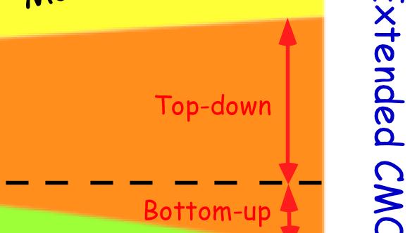

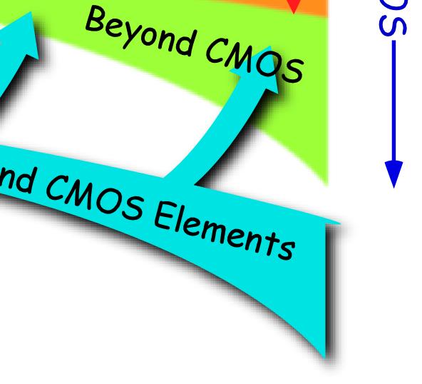
6 Evolution of Extended CMOS Existing technologies Elements ERD-WG in Japan New technologies Beyond CMOS year 6
7 シリコンナノワイヤトランジスタの研究 7
8 シリコンナノワイヤトランジスタの定義 本研究開発における定義 * ワイヤ径が 15nm 程度以下のナノワイヤチャネルを有するトランジスタで, 量子閉じ込め効果等のナノ構造特有の物理現象によってデバイス特性が変化するトランジスタ. * 経済産業省 NEDO ナノエレクトロニクスプロジェクト東京大学 東芝研究開発センター 8
 nfet と pfet の量子効果 (2001 IEDM) ナノワイヤを用いた NVM (2002 IEDM) 量子効果によるばらつき (2006 IEDM) ナノワイヤnFETの移動度 (2008 VLSI) ナノワイヤnFETの移動度 (2008 IEDM) 9")
9 研究実績 極薄 SOI トランジスタ シリコンナノワイヤトランジスタ pfet で移動度向上 (2005 VLSI) nfet で移動度向上 (2005 IEDM) ひずみの効果 (2007 IEDM) pmos の移動度 (2008 IEDM) 量子効果を室温観察 (1999 IEDM) nfet と pfet の量子効果 (2001 IEDM) ナノワイヤを用いた NVM (2002 IEDM) 量子効果によるばらつき (2006 IEDM) ナノワイヤnFETの移動度 (2008 VLSI) ナノワイヤnFETの移動度 (2008 IEDM) 9
![ナノスケール MOSFET における量子効果 - バルク MOSFET [1] 高濃度チャネルにおいて表面量子化 - 極薄 SOI MOSFET [2] 酸化膜による量子閉じ込め - ナノワイヤ MOSFET 幅方向にも量子閉じ込め](/docs-images/103/158061549/images/10-1.jpg "室温でも量子閉じ込め効果により Vth が上昇 [1] Y. Ohkura, Solid- State Electronics, Vol. 33, p. 1581, 1990. [2] Y. Omura, et al., IEEE EDL, Vol. 18, p.")
10 ナノスケール MOSFET における量子効果 - バルク MOSFET [1] 高濃度チャネルにおいて表面量子化 - 極薄 SOI MOSFET [2] 酸化膜による量子閉じ込め - ナノワイヤ MOSFET 幅方向にも量子閉じ込め 室温でも量子閉じ込め効果により Vth が上昇 [1] Y. Ohkura, Solid- State Electronics, Vol. 33, p. 1581, [2] Y. Omura, et al., IEEE EDL, Vol. 18, p. 190,
11 量子効果による正孔移動度の向上 280 same as bulk μeff [cm 2 /Vs] bulk, <110> mobility enhancement, <110> pmos N inv =3x10 12 cm t SOI [nm] G. Tsutsui et al. VLSI Symposium,
12 目次 1. ナノワイヤ nfet における移動度 Presented in 2008 VLSI Symposium. Presented in 2008 IEDM. 2. ナノワイヤ pfet における移動度 Presented in 2009 VLSI Symposium. 12
13 ナノワイヤ nfet における移動度 13
14 作製プロセス SiO 2 EB Resist SOI BOX Mesa EBL Dry Etching SC1 BHF Source 3D Structure Drain BOX BOX NW Narrowing BHF BOX 14
15 サブスレッショルド特性 Abs(Id) (A) 1E-3 1E-5 1E-7 1E-9 1E-11 [100]/ Num=1000 pfet T SOI =19nm L g =3μm narrower nfet T SOI =22nm L g =3μm Vd =10mV 1E Vg (V) S.S. (mv/dec.) pfet nfet average:61.7 mv/dec average:61.2 mv/dec L g =3μm W NW (nm) J. Chen et al., VLSI Technology Symposium, p. 32,
16 ナノワイヤの数 Id L g =3μm L g =4μm L g =3μm L g =4μm 3 C gc (pf)@vg=3v (a) NWs Number (b) NWs Number J. Chen et al., VLSI Technology Symposium, p. 32,
17 2 つの異なるワイヤ長で測定 Device Design: Nanowire of different Length Capacitance (pf) L=3μm Cg-Vg [100] NWs-nMOS W NW =40nm 1 L=3um L=4um Gate Voltage (V) ΔC g I d [A] L=4μm Id-Vg [100] NWs-nMOS L=3um 0.03 L=4um Gate Voltage [V] * A. Toriumi et al, IEDM, Tech. Dig., 671, I d [ma] 17
18 移動度の導出 μ eff = (Lm,1 L m,2 ) ( ) (C V gc,1 C gc,2)dvg ds Ids,1 Ids, [100] NWs-nFET μ eff (cm 2 /Vs) Tsoi=30nm W NW =40nm double L m method split CV method L g =3μm L g =4μm N inv (10 12 cm -2 ) * A. Toriumi et al, IEDM, Tech. Dig., 671,
19 面と 2 つの方向 j [100] j [110] 19
20 nfet の移動度 μ eff (cm 2 /Vs) [100] NWs-nFETs T soi =30nm [100] NWs-nFET UTB W NW :48nm Tsoi=30nm Tsoi=30nm 40nm 26nm 21nm 15nm 7nm j //[100] 3D-view cross-view 1 10 N inv (10 12 cm -2 ) J. Chen et al., VLSI Symposium, p. 32,
21 μ eff (cm 2 /Vs) nfet の移動度 [110] NWs-nFETs T soi =18nm [110] NWs-nFET UTB Tsoi=30nm Tsoi=18nm W NW :48nm 40nm 26nm 21nm j //[110] 3D-view cross-view 1 10 N inv (10 12 cm -2 ) J. Chen et al., VLSI Symposium, p. 32,
22 nfet の移動度まとめ Width Dependence Side-surface Dependence μ eff (cm 2 /Vs) [100] Tsoi=30nm [100] Tsoi=22nm [110] Tsoi=18nm N inv =5x10 12 cm W NW (nm) μ eff degradation in narrower NW μ eff [110] / μ eff [100] j W nw 40nm [110] T soi N inv :5x10 12 cm nm 21 nm Tsoi/(Tsoi+W nw ) Linear side surfaces contribution Side surface orientation plays the key role in NWs mobility J. Chen et al., VLSI Symposium, p. 32,
23 と j [100] j [110] [110]- and [100]-NWs are fabricated on the same SOI chip for better comparisons j [100] j [110] 23
24 nfet の移動度 Lower mobility in NWs than in bulk Si Small mobility degradation as diminishing W nw 1000 μ eff [cm 2 /Vs] 100 [100]/ NWs nfets T soi =18nm 1x10 12 [*] H. Irie et al., IEDM, p.225, ref [*] bulk [100]/ W nw : 30nm W nw : 46nm N inv [cm -2 ] 8x10 12 j //[100] 3D-view cross-view J. Chen et al., IEDM, p. 757,
25 nfet の移動度 Higher mobility in NWs than in bulk Si at low N inv Mobility improvement in narrower W nw 1000 μ eff [cm 2 /Vs] 100 [110]/ NWs nfets T soi =18nm W nw : 46nm 1x10 12 [*] H. Irie et al., IEDM, p.225, W nw : 30nm N inv [cm -2 ] ref [*] bulk [100]/ ref [*] bulk [110]/ 8x D-view cross-view j //[110] J. Chen et al., IEDM, p. 757,
26 nfet の移動度まとめ μ eff [cm 2 /Vs] N inv =1.5x10 12 cm -2 [110]-NWs [100]-NWs W nw [nm] N inv =1.5x10 12 cm μ eff [110]/μ eff [100] In wide W nw, μ eff in [100]-NWs is higher than that in [110]-NWs. As reducing W nw, μ eff in [110]-NWs is improved and even higher than that in [100]-NWs. j [100] j [110] J. Chen et al., IEDM, p. 757,
27 ナノワイヤ pfet における移動度 27
28 と における正孔移動度 μ h (cm 2 /Vs) /<110> x1.3 /<100> x1.6 /<110> Si 300K N inv (cm -2 ) Ken Shimizu et al., IEDM,
29 における正孔移動度 Hole mobility in pfets [110]/ >> [100]/ > j [110] j [100] [100]-direction [110]-direction middle µ [100] NW middle µ lowest µ highest µ [110] NW 29
![[100]/ の正孔移動度 Hole Mobility [cm 2 /vs] 300 200 100 [100]/ NWs pfets T SOI =18nm [100]/ universal [100]/ UTB W nw =18nm W nw =55nm Approaching to bulk Si 1 10 N inv [10 12 cm -2](/docs-images/103/158061549/images/30-1.jpg "] j //[100] 3D-view middle µ cross-view Hole in narrow NWs approaches to universal curve [*] H. Irie et al., IEDM, p.225, 2004. middle µ J. Chen et al., VLSI Symposium, 2009.")
30 [100]/ の正孔移動度 Hole Mobility [cm 2 /vs] [100]/ NWs pfets T SOI =18nm [100]/ universal [100]/ UTB W nw =18nm W nw =55nm Approaching to bulk Si 1 10 N inv [10 12 cm -2 ] j //[100] 3D-view middle µ cross-view Hole in narrow NWs approaches to universal curve [*] H. Irie et al., IEDM, p.225, middle µ J. Chen et al., VLSI Symposium,
31 [110]/ の正孔移動度 Hole Mobility [cm 2 /vs] [110]/ NWs pfets T SOI =18nm [110]/ universal [110]/ UTB W nw =68, 42, 25nm 1 10 N inv [10 12 cm -2 ] 2.4x [110]/ universal j //[110] 3D-view highest µ lowest µ cross-view High hole mobility in narrow NWs at high N inv [*] H. Irie et al., IEDM, p.225, J. Chen et al., VLSI Symposium,
![チャネル方向依存性 Hole Mobility [cm 2 /vs] 300 200 100 solid: N inv =5x10 12 cm -2 open: N inv =1x10 13 cm -2 [110] [100] 1.4x [100]/ bulk Si univ.](/docs-images/103/158061549/images/32-0.jpg "@ N inv =1x10 13 cm -2 [*] middle µ middle µ [100]-direction highest µ lowest µ 15 30 45 60 75 W nw [nm] [110]-direction [*] H. Irie et al., IEDM, p.225, 2004. J.")
32 チャネル方向依存性 Hole Mobility [cm 2 /vs] solid: N inv =5x10 12 cm -2 open: N inv =1x10 13 cm -2 [110] [100] 1.4x [100]/ bulk Si N inv =1x10 13 cm -2 [*] middle µ middle µ [100]-direction highest µ lowest µ W nw [nm] [110]-direction [*] H. Irie et al., IEDM, p.225, J. Chen et al., VLSI Symposium,
33 移動度の Ninv 依存性 μ narrow /μ wide 1 [100] NW 68nm/25nm approaching to wide NWs 0.55 NW pfets Negligible degradation 55nm/18nm [100] [110] 0.93 [110] NW N inv [10 12 cm -2 ] Large degradation Small degradation J. Chen et al., VLSI Symposium,
34 面におけるサブバンドエネルギー Subband Energy [ev] Why high hole mobility? Surface Surface Fs [MV/cm] ΔE [ev] Fs [MV/cm] anisotropic m* eff F s Increase ΔE Hole Population on surface increase turns to be much more dominant in [110] NWs at higher N inv [*] M.V. Fischetti et al., J. App. Phys. 94(2), p1079,


35 ナノワイヤーにおけるコーナー効果 No mobility degradation at high field When Electric Field is applied Low Field Middle Field High Field Less effect by side surface Less width dependence of µ Hole Distribution in [110] Nanowire [*] T soi 12nm W nw 12nm 6nm 3nm More population in even at the corners µ is mainly dominated by. [*] N. Neophytou et al. Nano. Lett. p. 623,
36 と j [100] j [110] To be presented in 2010 VLSI Technology Symposium. j [100] j [110] 36
37 まとめ 1. ナノワイヤ nfet では, 側壁効果が移動度に大きく影響する. 2. ナノワイヤ pfet では, 側壁効果ではなく, 閉じ込めの効果等が移動度に影響する. 本研究の一部は,NEDO のプロジェクト ナノエレクトロニクス半導体材利用 新構造なの電子デバイス技術開発 の援助を受けた. 37
untitled
 /Si FET /Si FET Improvement of tunnel FET performance using narrow bandgap semiconductor silicide Improvement /Si hetero-structure of tunnel FET performance source electrode using narrow bandgap semiconductor
untitled
 213 74 AlGaN/GaN Influence of metal material on capacitance for Schottky-gated AlGaN/GaN 1, 2, 1, 2, 2, 2, 2, 2, 2, 2, 1, 1 1 AlGaN/GaN デバイス ① GaNの優れた物性値 ② AlGaN/GaN HEMT構造 ワイドバンドギャップ半導体 (3.4eV) 絶縁破壊電界が大きい
PowerPoint プレゼンテーション
 STRJ ITRS 2003 LSI 2004.3.4. MIRAI 100nmCMOS - Si SOI CMOS SOI MOSFET CMOS 100nmCMOS trade-off Sub 100 nm CMOS trade-off x j (ext. conc.) Nsub Vdd Vth design EOT S or Si Nsub EOT something S/D EOT SiGe
スライド 1
 High-k & Selete 1 2 * * NEC * # * # # 3 4 10 Si/Diamond, Si/SiC, Si/AlOx, Si Si,,, CN SoC, 2007 2010 2013 2016 2019 Materials Selection CZ Defectengineered SOI: Bonded, SIMOX, SOI Emerging Materials Various
スライド 1
 Front End Processes FEP WG - - NEC 1 ITRS2006 update 2 ITRS vs. 2-1 FET 2-2 Source Drain Extension 2-3 Si-Silicide 2-4 2-5 1 , FEP Front End Processes Starting Materials: FEP Si,, SOI SOI: Si on Insulator,
untitled
 MOSFET 17 1 MOSFET.1 MOS.1.1 MOS.1. MOS.1.3 MOS 4.1.4 8.1.5 9. MOSFET..1 1.. 13..3 18..4 18..5 0..6 1.3 MOSFET.3.1.3. Poon & Yau 3.3.3 LDD MOSFET 5 3.1 3.1.1 6 3.1. 6 3. p MOSFET 3..1 8 3.. 31 3..3 36
untitled
 Tokyo Institute of Technology high-k/ In.53 Ga.47 As MOS - Defect Analysis of high-k/in.53 G a.47 As MOS Capacitor using capacitance voltage method,,, Darius Zade,,, Parhat Ahmet,,,,,, ~InGaAs high-k ~
スライド 1
 Matsuura Laboratory SiC SiC 13 2004 10 21 22 H-SiC ( C-SiC HOY Matsuura Laboratory n E C E D ( E F E T Matsuura Laboratory Matsuura Laboratory DLTS Osaka Electro-Communication University Unoped n 3C-SiC
MOSFET HiSIM HiSIM2 1
 MOSFET 2007 11 19 HiSIM HiSIM2 1 p/n Junction Shockley - - on-quasi-static - - - Y- HiSIM2 2 Wilson E f E c E g E v Bandgap: E g Fermi Level: E f HiSIM2 3 a Si 1s 2s 2p 3s 3p HiSIM2 4 Fermi-Dirac Distribution
PowerPoint プレゼンテーション
 Drain Voltage (mv) 4 2 0-2 -4 0.0 0.2 0.4 0.6 0.8 1.0 Gate Voltage (V) Vds [V] 0.2 0.1 0.0-0.1-0.2-10 -8-6 -4-2 0 Vgs [V] 10 1000 1000 1000 1000 (LSI) Fe Catalyst Fe Catalyst Carbon nanotube 1~2 nm
電子回路I_4.ppt
 電子回路 Ⅰ 第 4 回 電子回路 Ⅰ 5 1 講義内容 1. 半導体素子 ( ダイオードとトランジスタ ) 2. 基本回路 3. 増幅回路 電界効果トランジスタ (FET) 基本構造 基本動作動作原理 静特性 電子回路 Ⅰ 5 2 半導体素子 ( ダイオードとトランジスタ ) ダイオード (2 端子素子 ) トランジスタ (3 端子素子 ) バイポーラトランジスタ (Biolar) 電界効果トランジスタ
untitled
 2013 74 Tokyo Institute of Technology AlGaN/GaN C Annealing me Dependent Contact Resistance of C Electrodes on AlGaN/GaN, Tokyo Tech.FRC, Tokyo Tech. IGSSE, Toshiba, Y. Matsukawa, M. Okamoto, K. Kakushima,
DA DA シンポジウム DAS25 Design Automation Symposium 25/8/26 Gate Gate Source n Drain n Source n BOX Drain n 2 SOI 2 3 TCAD 4 PHITSTCAD (LSI)
") DA DA シンポジウム 25 27 DAS25 Design Automation Symposium 25/8/26 28nm UTBB FDSOI SOI 28nm UTBB FDSOI Analysis of Soft Error Rates in a 28nm UTBB FDSOI Structure by DeviceLevel Simulation Shigehiro Umehara
DA DA シンポジウム 25 27 DAS25 Design Automation Symposium 25/8/26 28nm UTBB FDSOI SOI 28nm UTBB FDSOI Analysis of Soft Error Rates in a 28nm UTBB FDSOI Structure by DeviceLevel Simulation Shigehiro Umehara
untitled
 20101221JST (SiC - Buried Gate Static Induction Transistor: SiC-BGSIT) SOURCE GATE N source layer p + n p + n p + n p+ n drift layer n + substrate DRAIN SiC-BGSIT (mωcm 2 ) 200 100 40 10 4 1 Si limit
untitled
 ITRS2005 DFM STRJ : () 1 ITRS STRJ ITRS2005DFM STRJ DFM ITRS: International Technology Roadmap for Semiconductors STRJ: Semiconductor Technology Roadmap committee of Japan 2 ITRS STRJ 1990 1998 2000 2005
( ) : 1997
 : 1997") ( ) 2008 2 17 : 1997 CMOS FET AD-DA All Rights Reserved (c) Yoichi OKABE 2000-present. [ HTML ] [ PDF ] [ ] [ Web ] [ ] [ HTML ] [ PDF ] 1 1 4 1.1..................................... 4 1.2..................................
( ) 2008 2 17 : 1997 CMOS FET AD-DA All Rights Reserved (c) Yoichi OKABE 2000-present. [ HTML ] [ PDF ] [ ] [ Web ] [ ] [ HTML ] [ PDF ] 1 1 4 1.1..................................... 4 1.2..................................
PowerPoint プレゼンテーション
 第 61 回応用物理学会 青山学院大学相模原キャンパス 春季学術講演会 2014 年 3 月 18 日 ( 火曜日 ) La 2 O 3 /InGaAs 界面ラフネスに及ぼす ALD プロセスの影響 Impact of ALD process on La 2 O 3 /InGaAs interface roughness 大嶺洋 1,Dariush Hassan Zadeh 1, 角嶋邦之 2, 片岡好則
Microsoft PowerPoint - semi_ppt07.ppt
 半導体工学第 9 回目 / OKM 1 MOSFET の動作原理 しきい電圧 (V( TH) と制御 E 型と D 型 0 次近似によるドレイン電流解析 半導体工学第 9 回目 / OKM 2 電子のエネルギーバンド図での考察 金属 (M) 酸化膜 (O) シリコン (S) 熱平衡でフラットバンド 伝導帯 E c 電子エネルギ シリコンと金属の仕事関数が等しい 界面を含む酸化膜中に余分な電荷がない
支援財団研究活動助成 生体超分子を利用利用した 3 次元メモリデバイスメモリデバイスの研究 奈良先端科学技術大学院大学物質創成科学研究科小原孝介
 2009.3.10 支援財団研究活動助成 生体超分子を利用利用した 3 次元メモリデバイスメモリデバイスの研究 奈良先端科学技術大学院大学物質創成科学研究科小原孝介 研究背景研究背景研究背景研究背景データデータデータデータの種類種類種類種類データデータデータデータの保存保存保存保存パソコンパソコンパソコンパソコンパソコンパソコンパソコンパソコンデータデータデータデータデータデータデータデータ音楽音楽音楽音楽音楽音楽音楽音楽写真写真写真写真記録媒体記録媒体記録媒体記録媒体フラッシュメモリフラッシュメモリフラッシュメモリフラッシュメモリ動画動画動画動画
スライド 1
 STRJ WS: March 9, 2006, 0.35µm 0.8µm 0.3µm STRJ WS: March 9, 2006, 2 0.35µm Lot-to-Lot, Wafer-to-Wafer, Die-to-Die(D2D) D2D 0.8µm (WID: Within Die) D2D vs. WID 0.3µm D2Dvs. WID STRJ WS: March 9, 2006,
1 薄膜 BOX-SOI (SOTB) を用いた 2M ビット SRAM の超低電圧 0.37V 動作を実証 大規模集積化に成功 超低電圧 超低電力 LSI 実現に目処 独立行政法人新エネルギー 産業技術総合開発機構 ( 理事長古川一夫 / 以下 NEDOと略記 ) 超低電圧デバイス技術研究組合(
 を用いた 2M ビット SRAM の超低電圧 0.37V 動作を実証 大規模集積化に成功 超低電圧 超低電力 LSI 実現に目処 独立行政法人新エネルギー 産業技術総合開発機構 ( 理事長古川一夫 / 以下 NEDOと略記 ) 超低電圧デバイス技術研究組合(") 1 薄膜 BOX-SOI (SOTB) を用いた 2M ビット SRAM の超低電圧 0.37V 動作を実証 大規模集積化に成功 超低電圧 超低電力 LSI 実現に目処 独立行政法人新エネルギー 産業技術総合開発機構 ( 理事長古川一夫 / 以下 NEDOと略記 ) 超低電圧デバイス技術研究組合( 理事長 : 豊木則行 / 以下 LEAP と略記 ) と国立大学法人東京大学は このたび マイコン等に使われる論理集積回路の大幅な省エネ化を可能とする
1 薄膜 BOX-SOI (SOTB) を用いた 2M ビット SRAM の超低電圧 0.37V 動作を実証 大規模集積化に成功 超低電圧 超低電力 LSI 実現に目処 独立行政法人新エネルギー 産業技術総合開発機構 ( 理事長古川一夫 / 以下 NEDOと略記 ) 超低電圧デバイス技術研究組合( 理事長 : 豊木則行 / 以下 LEAP と略記 ) と国立大学法人東京大学は このたび マイコン等に使われる論理集積回路の大幅な省エネ化を可能とする
10 IDM NEC
 No.29 1 29 SEAJ SEAJ 2 3 63 1 1 2 2002 2003 6 News 9 IEDM 11 13 15 16 17 10 IDM NEC 3 12 3 10 10 2 3 3 20 110 1985 1995 1988 912001 1 1993 95 9798 199010 90 200 2 1950 2 1950 3 1311 10 3 4 4 5 51929 3
Natural Convection Heat Transfer in a Horizontal Porous Enclosure with High Porosity Yasuaki SHIINA*4, Kota ISHIKAWA and Makoto HISHIDA Nuclear Applie
 Natural Convection Heat Transfer in a Horizontal Porous Enclosure with High Porosity Yasuaki SHIINA*4, Kota ISHIKAWA and Makoto HISHIDA Nuclear Applied Heat Technology Division, Japan Atomic Energy Agency,
untitled
 Recent Our Activities in Si FET Research November 3, 29 IIT Madras, India Hiroshi Iwai Tokyo Institute of Technology Europe 78 Asia 847 North America 12 Africa 16 Oceania 5 South America 24 Total 982 (As
PowerPoint Presentation
 半導体電子工学 II 神戸大学工学部 電気電子工学科 12/08/'10 半導体電子工学 Ⅱ 1 全体の内容 日付内容 ( 予定 ) 備考 1 10 月 6 日半導体電子工学 I の基礎 ( 復習 ) 11/24/'10 2 10 月 13 日 pn 接合ダイオード (1) 3 10 月 20 日 4 10 月 27 日 5 11 月 10 日 pn 接合ダイオード (2) pn 接合ダイオード (3)
PowerPoint プレゼンテーション
 1 45nm 2 2004 2007 2010 90* 65 45 4 10 25 * 100 10001 H16 45 2001-2003 2004-2007 65 45 MIRAI 3 Cu n+ n+ p+ p+ p n nmos pmos ITRS 2004 2007 2010 2013 2016 3.5 k 3.0 2.5 2.0 ITRS2001 ITRS2003 Low-k 1.5 1.0
テストコスト抑制のための技術課題-DFTとATEの観点から
 2 -at -talk -talk -drop 3 4 5 6 7 Year of Production 2003 2004 2005 2006 2007 2008 Embedded Cores Standardization of core Standard format Standard format Standard format Extension to Extension to test
日立金属技報 Vol.34
 Influence of Misorientation Angle between Adjacent Grains on Magnetization Reversal in Nd-Fe-B Sintered Magnet Tomohito Maki Rintaro Ishii Mitsutoshi Natsumeda Takeshi Nishiuchi Ryo Uchikoshi Masaaki Takezawa
Original (English version) Copyright 2001 Semiconductor Industry Association All rights reserved ITRS 2706 Montopolis Drive Austin, Texas
 Copyright 2001 Semiconductor Industry Association All rights reserved ITRS 2706 Montopolis Drive Austin, Texas") INTERNATIONAL TECHNOLOGY ROADMAP FOR SEMICONDUCTORS 2001 EDITION EECA, European Electronic Component Manufacturers Association () JEITA, Japan Electronics and Information Technology Industries Association
INTERNATIONAL TECHNOLOGY ROADMAP FOR SEMICONDUCTORS 2001 EDITION EECA, European Electronic Component Manufacturers Association () JEITA, Japan Electronics and Information Technology Industries Association
パナソニック技報
 Panasonic Technical Journal Vol. 63 No. 1 May 2017 Development of Simultaneous-Capture Wide-dynamic-range Technology and Global Shutter Technology for Organic Photoconductive Film Image Sensor Masashi
ナノテクノロジ
 Nanotechnology 10 1 HEMT 201 2000 12 Abstract Since former President Clinton announced the National Nanotechnology Initiative, nanotechnology has become a well-known field. It has attracted much attention
藤村氏(論文1).indd
.indd") Nano-pattern profile control technology using reactive ion etching Megumi Fujimura, Yasuo Hosoda, Masahiro Katsumura, Masaki Kobayashi, Hiroaki Kitahara Kazunobu Hashimoto, Osamu Kasono, Tetsuya Iida,
Nano-pattern profile control technology using reactive ion etching Megumi Fujimura, Yasuo Hosoda, Masahiro Katsumura, Masaki Kobayashi, Hiroaki Kitahara Kazunobu Hashimoto, Osamu Kasono, Tetsuya Iida,
Microsoft PowerPoint - semi_ppt07.ppt [互換モード]
![Microsoft PowerPoint - semi_ppt07.ppt [互換モード]](/thumbs/94/122068205.jpg "Microsoft PowerPoint - semi_ppt07.ppt [互換モード]") 1 MOSFETの動作原理 しきい電圧 (V TH ) と制御 E 型とD 型 0 次近似によるドレイン電流解析 2 電子のエネルギーバンド図での考察 理想 MOS 構造の仮定 : シリコンと金属の仕事関数が等しい 界面を含む酸化膜中に余分な電荷がない 金属 (M) 酸化膜 (O) シリコン (S) 電子エ金属 酸化膜 シリコン (M) (O) (S) フラットバンド ネルギー熱平衡で 伝導帯 E
1 MOSFETの動作原理 しきい電圧 (V TH ) と制御 E 型とD 型 0 次近似によるドレイン電流解析 2 電子のエネルギーバンド図での考察 理想 MOS 構造の仮定 : シリコンと金属の仕事関数が等しい 界面を含む酸化膜中に余分な電荷がない 金属 (M) 酸化膜 (O) シリコン (S) 電子エ金属 酸化膜 シリコン (M) (O) (S) フラットバンド ネルギー熱平衡で 伝導帯 E
 hν 688 358 979 309 308.123 Hz α α α α α α No.37 に示す Ti Sa レーザーで実現 術移転も成功し 図 9 に示すよ うに 2 時間は連続測定が可能な システムを実現した Advanced S o l i d S t a t e L a s e r s 2016, JTu2A.26 1-3. 今後は光周波 数比計測装置としてさらに改良 を加えていくとともに
LMV851/LMV852/LMV854 8 MHz Low Power CMOS, EMI Hardened Operational Amplifi(jp)
") LMV851,LMV852,LMV854 LMV851/LMV852/LMV854 8 MHz Low Power CMOS, EMI Hardened Operational Amplifiers Literature Number: JAJSAM3 LMV851/LMV852/LMV854 8MHz CMOS EMI LMV851/LMV852/LMV854 CMOS IC 40 125 LMV851/
LMV851,LMV852,LMV854 LMV851/LMV852/LMV854 8 MHz Low Power CMOS, EMI Hardened Operational Amplifiers Literature Number: JAJSAM3 LMV851/LMV852/LMV854 8MHz CMOS EMI LMV851/LMV852/LMV854 CMOS IC 40 125 LMV851/
単位、情報量、デジタルデータ、CPUと高速化 ~ICT用語集~
 CPU ICT mizutani@ic.daito.ac.jp 2014 SI: Systèm International d Unités SI SI 10 1 da 10 1 d 10 2 h 10 2 c 10 3 k 10 3 m 10 6 M 10 6 µ 10 9 G 10 9 n 10 12 T 10 12 p 10 15 P 10 15 f 10 18 E 10 18 a 10 21
Microsoft PowerPoint 修論発表_細田.ppt
 0.0.0 ( 月 ) 修士論文発表 Carrier trasort modelig i diamods ( ダイヤモンドにおけるキャリヤ輸送モデリング ) 物理電子システム創造専攻岩井研究室 M688 細田倫央 Tokyo Istitute of Techology パワーデバイス基板としてのダイヤモンド Proerty (relative to Si) Si GaAs SiC Ga Diamod
スライド 1
 SoC -SWG ATE -SWG 2004 2005 1 SEAJ 2 VLSI 3 How can we improve manageability of the divergence between validation and manufacturing equipment? What is the cost and capability optimal SOC test approach?
PowerPoint プレゼンテーション
 実空間差分法に基づく 第一原理電子構造 量子輸送特性計算 09/05/15 大阪大学大学院工学研究科小野倫也 Real-space first-principles calculation code The grand-state electronic structure is obtained by solving the Schrödinger (Kohn-Sham) equation 1 2
untitled
 CAPEC, 2009 6 16 June 16, 2009 Page 1 CAPEC EMS 1. EMS USA EU 2. EMS 3. EMS 4. EMS 5. CAPEC 6. EMS June 16, 2009 Page 2 EMS EC 3 EMS EMS EMS EMS CAPEC EMS CAPEC EMS EMS June 16, 2009 Page 3 EU EU EC 1997/67/EC
LM6172 デュアル高速低消費電力、低歪み電圧帰還アンプ
 Dual High Speed, Low Power, Low Distortion, Voltage Feedback Amplifiers Literature Number: JAJS854 100MHz 3000V/ s 50mA 2.3mA/ 15V ADSL 5V VIP III (Vertically Integrated PNP) LM6171 Dual High Speed, Low
2 3 v v S i i L L S i i E i v L E i v 3. L urren (A) approx. 60% E = V = 0 Ω L = 00 mh urren (A) app
 approx. 60% E = V = 0 Ω L = 00 mh urren (A) app") 3 ON ON L * 3. v() = i() (3.) 3.2 L 3. L = 0 S i() = i () = i L () v () L v L () = 0 L v () = i(), (3.4) v L () = L d i(). (3.5) d v () + v L () = E, (3.6) i () = i L () = i(). (3.7) L d i() + i() = E.
3 ON ON L * 3. v() = i() (3.) 3.2 L 3. L = 0 S i() = i () = i L () v () L v L () = 0 L v () = i(), (3.4) v L () = L d i(). (3.5) d v () + v L () = E, (3.6) i () = i L () = i(). (3.7) L d i() + i() = E.
 Time and Temperature Dependence of Recovery Behavior of Residual Strains in Largely Deformed Glassy Poly (Methyl Methacrylate) by Shin'ya YOSHIOKA*, Ryoji NAKAGAWA** and Yukuo NANZAI* Time and temperature
PowerPoint Presentation
 半導体電子工学 II 神戸大学工学部電気電子工学科 小川真人 09/01/21 半導体電子工学 II 日付内容 ( 予定 ) 備考 1 10 月 1 日半導体電子工学 I の基礎 ( 復習 ) 2 10 月 8 日半導体電子工学 I の基礎 ( 復習 ) 3 10 月 15 日 pn 接合ダイオード (1) 4 10 月 22 日 pn 接合ダイオード (2) 5 10 月 29 日 pn 接合ダイオード
Microsoft PowerPoint - 14.菅谷修正.pptx
 InGaAs/系量子ドット太陽電池の作製 革新デバイスチーム 菅谷武芳 電子 バンド3:伝導帯 E3 E3 E 正孔 バンド:中間バンド 量子ドット超格子 ミニバンド 量子ドットの井戸型 ポテンシャル バンド:価電子帯 量子ドット太陽電池のバンド図 6%を超える理想的な量子ドット太陽 電池実現には E3として1 9eVが必要 量子ドット超格子太陽電池 理論上 変換効率6%以上 集光 を採用 MBE
Microsoft PowerPoint - 4.1I-V特性.pptx
 4.1 I-V 特性 MOSFET 特性とモデル 1 物理レベルの設計 第 3 章までに システム~ トランジスタレベルまでの設計の概要を学んだが 製造するためには さらに物理的パラメータ ( 寸法など ) が必要 物理的パラメータの決定には トランジスタの特性を理解する必要がある ゲート内の配線の太さ = 最小加工寸法 物理的パラメータの例 電源配線の太さ = 電源ラインに接続されるゲート数 (
3次元LSI集積化技術
 3 LSI 3D LSI Integration Technology あらまし LSI 33DI LSI Si TSV Wafer on Wafer WOW 3 45 nm CMOS LSI FeRAM 10 m 200 3 LSI Abstract The conventional enhancement of LSIs based on Moore s Law is approaching its
PowerPoint プレゼンテーション
 冷却エレクトロニクス STJ 読み出し用 SOI 極低温アンプ TIAかけはし事業 簡単 便利な超伝導計測 ミニ研究会 2017 年 1 月 4 日 @ 物質 材料研究機構 (NIMS) 武内勇司 ( 筑波大 ) on behalf of COBAND collaboration 1 500pA/DIV Leakage CRVAVITY 製 Nb/Al-STJ 50 m sq. Nb/Al-STJ
Table 1. Reluctance equalization design. Fig. 2. Voltage vector of LSynRM. Fig. 4. Analytical model. Table 2. Specifications of analytical models. Fig
 Mover Design and Performance Analysis of Linear Synchronous Reluctance Motor with Multi-flux Barrier Masayuki Sanada, Member, Mitsutoshi Asano, Student Member, Shigeo Morimoto, Member, Yoji Takeda, Member
42 1 Fig. 2. Li 2 B 4 O 7 crystals with 3inches and 4inches in diameter. Fig. 4. Transmission curve of Li 2 B 4 O 7 crystal. Fig. 5. Refractive index
 MEMOIRS OF SHONAN INSTITUTE OF TECHNOLOGY Vol. 42, No. 1, 2008 Li 2 B 4 O 7 (LBO) *, ** * ** ** Optical Scatterer and Crystal Growth Technology of LBO Single Crystal For Development with Optical Application
B1 Ver ( ), SPICE.,,,,. * : student : jikken. [ ] ( TarouOsaka). (, ) 1 SPICE ( SPICE. *1 OrCAD
![B1 Ver ( ), SPICE.,,,,. * : student : jikken. [ ] ( TarouOsaka). (, ) 1 SPICE ( SPICE. *1 OrCAD](/thumbs/101/152175529.jpg "B1 Ver ( ), SPICE.,,,,. * : student : jikken. [ ] ( TarouOsaka). (, ) 1 SPICE ( SPICE. *1 OrCAD") B1 er. 3.05 (2019.03.27), SPICE.,,,,. * 1 1. 1. 1 1.. 2. : student : jikken. [ ] ( TarouOsaka). (, ) 1 SPICE ( SPICE. *1 OrCAD https://www.orcad.com/jp/resources/orcad-downloads.. 1 2. SPICE 1. SPICE Windows
B1 er. 3.05 (2019.03.27), SPICE.,,,,. * 1 1. 1. 1 1.. 2. : student : jikken. [ ] ( TarouOsaka). (, ) 1 SPICE ( SPICE. *1 OrCAD https://www.orcad.com/jp/resources/orcad-downloads.. 1 2. SPICE 1. SPICE Windows
PowerPoint プレゼンテーション
 () 増幅回路の周波数特性 Frequency characteristic of amplifier circuit (2) 増幅回路の周波数特性 Frequency characteristic of amplifier circuit MOS トランジスタの高周波モデル High-frequency model for MOS FET ゲート酸化膜は薄いので G-S, G-D 間に静電容量が生じる
原稿.indd
 OTEC 18(2013),5968 小型の波浪発電を想定した浮体運動の最大化を目的とした浮体形状に関する研究 59 *1 *1 *2 Studies on the floating body shape to maximize the kinetic energy that are intended to be small wave power generator Shunya NISHIZAWA
<95DB8C9288E397C389C88A E696E6462>
 2011 Vol.60 No.2 p.138 147 Performance of the Japanese long-term care benefit: An International comparison based on OECD health data Mie MORIKAWA[1] Takako TSUTSUI[2] [1]National Institute of Public Health,
DA DA シンポジウム DAS2015 Design Automation Symposium 2015/8/26 65nm FD-SOI SOI (Sillicon On Insulatar) 65nm FD-SOI (Fully-Depleted SOI) 1.4
 65nm FD-SOI (Fully-Depleted SOI) 1.4") 65nm FD-SOI SOI (Sillicon On Insulatar) 65nm FD-SOI (Fully-Depleted SOI).4 FD-SOI 8 FD-SOI Measurements and Evaluations of Soft error induced by Antenna Diode in 65 nm and SOTB Processes Eiji Sonezaki
65nm FD-SOI SOI (Sillicon On Insulatar) 65nm FD-SOI (Fully-Depleted SOI).4 FD-SOI 8 FD-SOI Measurements and Evaluations of Soft error induced by Antenna Diode in 65 nm and SOTB Processes Eiji Sonezaki
1-2 原子層制御量子ナノ構造のコヒーレント量子効果 Coherent Quantum Effects in Quantum Nano-structure with Atomic Layer Precision Mutsuo Ogura, Research Director of CREST Pho
 1-2 原子層制御量子ナノ構造のコヒーレント量子効果 Coherent Quantum Effects in Quantum Nano-structure with Atomic Layer Precision Mutsuo Ogura, Research Director of CREST Photonics Research Institute, AIST TBAs) AlGaAs/GaAs TBAs)
A comparative study of the team strengths calculated by mathematical and statistical methods and points and winning rate of the Tokyo Big6 Baseball Le
 Powered by TCPDF (www.tcpdf.org) Title 東京六大学野球リーグ戦において勝敗結果から計算する優勝チームと勝点 勝率との比較研究 Sub Title A comparative study of the team strengths calculated by mathematical and statistical methods and points and winning
c c SSIS10 10 10 1998 2001 SSIS 2001 LSI 2001 MIRAI NECASKA SELETE 21 5ISSCC LSI 2004 2004SSIS PR 60 70
 Encore SSIS 10 c c SSIS10 10 10 1998 2001 SSIS 2001 LSI 2001 MIRAI NECASKA SELETE 21 5ISSCC LSI 2004 2004SSIS PR 60 70 SSIS NOSIDE PR SSIS SSIS PR 2000 5SSIS SSIS 1 2001 5 8 3 2004 SSIS 1 2 SSIS 24 SSISPR
PowerPoint プレゼンテーション
 WG3 Front-End Processes(FEP) 新材料 新構造の導入を支える FEP 技術 水島一郎 ( 東芝 ) 内容 STRJ FEP のメンバー スコープ 今年度の活動 新材料 新構造の導入と FEP 技術 Si ウェーハ 450mm 化状況 まとめ 略号 FeRAM: Ferroelectric Random Access Memory HP: High Performance /
untitled
 1 2 3 4 5 130mm 32mm UV-irradiation UV-cationic cure UV-cationic cure UV-cationic cure Thermal cationic Reaction heat cure Thermal cationic Cation Reaction heat cure Cation (a) UV-curing of
Studies of Foot Form for Footwear Design (Part 9) : Characteristics of the Foot Form of Young and Elder Women Based on their Sizes of Ball Joint Girth
 : Characteristics of the Foot Form of Young and Elder Women Based on their Sizes of Ball Joint Girth") Studies of Foot Form for Footwear Design (Part 9) : Characteristics of the Foot Form of Young and Elder Women Based on their Sizes of Ball Joint Girth and Foot Breadth Akiko Yamamoto Fukuoka Women's University,
Studies of Foot Form for Footwear Design (Part 9) : Characteristics of the Foot Form of Young and Elder Women Based on their Sizes of Ball Joint Girth and Foot Breadth Akiko Yamamoto Fukuoka Women's University,
1. Introduction SOI(Silicon-On-Insulator) Monolithic Pixel Detector ~µm) 2
 Monolithic Pixel Detector ~µm) 2") Introduction TEG 2005.10.4 @KEK 1 1. Introduction SOI(Silicon-On-Insulator) Monolithic Pixel Detector ~µm) 2005.10.4 @KEK 2 SOI 2005.10.4 @KEK 3 SOI : Smart Cut (UNIBOND) by SOITEC Low-R Hi-R 2005.10.4
Introduction TEG 2005.10.4 @KEK 1 1. Introduction SOI(Silicon-On-Insulator) Monolithic Pixel Detector ~µm) 2005.10.4 @KEK 2 SOI 2005.10.4 @KEK 3 SOI : Smart Cut (UNIBOND) by SOITEC Low-R Hi-R 2005.10.4
Development of Induction and Exhaust Systems for Third-Era Honda Formula One Engines Induction and exhaust systems determine the amount of air intake
 Development of Induction and Exhaust Systems for Third-Era Honda Formula One Engines Induction and exhaust systems determine the amount of air intake supplied to the engine, and as such are critical elements
MOSFET 6-2 CMOS 6-2 TTL Transistor Transistor Logic ECL Emitter Coupled Logic I2L Integrated
 1 -- 7 6 2011 11 1 6-1 MOSFET 6-2 CMOS 6-2 TTL Transistor Transistor Logic ECL Emitter Coupled Logic I2L Integrated Injection Logic 6-3 CMOS CMOS NAND NOR CMOS 6-4 6-5 6-1 6-2 CMOS 6-3 6-4 6-5 c 2011 1/(33)
Conduction Mechanism at Low Temperature of 2-Dimensional Hole Gas at GaN/AlGaN Heterointerface (低温におけるGaN/AlGaN ヘテロ界面の2 次元正孔ガスの伝導機構)
") 2014/03/19 応用物理学会 2014 年春季学術講演会 コンダクタンス法による AlGaN/GaN ヘテロ 接合界面トラップに関する研究 Investigation on interface traps in AlGaN/GaN heterojunction by conductance method 劉璞誠 1, 竇春萌 2, 角嶋邦之 2, 片岡好則 2, 西山彰 2, 杉井信之 2,
2014/03/19 応用物理学会 2014 年春季学術講演会 コンダクタンス法による AlGaN/GaN ヘテロ 接合界面トラップに関する研究 Investigation on interface traps in AlGaN/GaN heterojunction by conductance method 劉璞誠 1, 竇春萌 2, 角嶋邦之 2, 片岡好則 2, 西山彰 2, 杉井信之 2,
1
 5-3 Photonic Antennas and its Application to Radio-over-Fiber Wireless Communication Systems LI Keren, MATSUI Toshiaki, and IZUTSU Masayuki In this paper, we presented our recent works on development of
I N S T R U M E N T A T I O N & E L E C T R I C A L E Q U I P M E N T Pressure-resistant gasket type retreat method effective bulk compressibility Fro
 Cable Gland This is the s to use for Cable Wiring in the hazardous location. It is much easier to install and maintenance and modification compared with Conduit Wiring with Sealing Fitting. The Standard
LM317A
 3 3 LM317A 3 LM317 1.2 37V 1.5A 3 IC 2 / IC AC IC 6 3 LM317 3-Terminal Adjustable Regulator LM117 19860710 33200 24060 11800 ds009063 Increase the print percent on all Typical Curves modified formatting
LM A High Efficiency Synchronous Switching Regulator (jp)
") LM2651 LM2651 1.5A High Efficiency Synchronous Switching Regulator Literature Number: JAJS632 LM2651 1.5A 1.5A High Efficiency Switching Regulator 2651 LM Dongyan Zhou 19980610 LM2651 100:1 (1.5A 15mA)
LM2651 LM2651 1.5A High Efficiency Synchronous Switching Regulator Literature Number: JAJS632 LM2651 1.5A 1.5A High Efficiency Switching Regulator 2651 LM Dongyan Zhou 19980610 LM2651 100:1 (1.5A 15mA)
第62巻 第1号 平成24年4月/石こうを用いた木材ペレット
 Bulletin of Japan Association for Fire Science and Engineering Vol. 62. No. 1 (2012) Development of Two-Dimensional Simple Simulation Model and Evaluation of Discharge Ability for Water Discharge of Firefighting
研究成果報告書
 10m 2m Ge Si BaF2 ZnSZnSe Sb-Ge-Sn-S IIR-SF1 1 2 Tungsten SilicideWSi WSi () IIR-SF 1 Sb-Ge-Sn-S 0.85~11μm2.710μm 253 C Al Al 220μm He-Cd laser 1 Exposure Photoresist WSi (a) 500 nm Development RIE WSi
03_委託テーマ発表資料(その2)(p.89-p.134).pdf
(p.89-p.134).pdf") 89 MEMS 2 / 5-0 0-20 90 3 Beyond-CMOS CNT CNT CNT NEC 4 NEDO (80 NEDO 2008.05 Nature Nanotechnology NEDO (8 22 CNT CNT NEDOPJ CNT NEDO M 3 5 Nature Nanotechnology 3, 289-294 (2008) 6 9 7 8 92 9 (!!! '!!!
89 MEMS 2 / 5-0 0-20 90 3 Beyond-CMOS CNT CNT CNT NEC 4 NEDO (80 NEDO 2008.05 Nature Nanotechnology NEDO (8 22 CNT CNT NEDOPJ CNT NEDO M 3 5 Nature Nanotechnology 3, 289-294 (2008) 6 9 7 8 92 9 (!!! '!!!
Microsoft PowerPoint - SDF2007_nakanishi_2.ppt[読み取り専用]
![Microsoft PowerPoint - SDF2007_nakanishi_2.ppt[読み取り専用]](/thumbs/94/118227082.jpg "Microsoft PowerPoint - SDF2007_nakanishi_2.ppt[読み取り専用]") ばらつきの計測と解析技術 7 年 月 日設計基盤開発部先端回路技術グループ中西甚吾 内容. はじめに. DMA(Device Matrix Array)-TEG. チップ間 チップ内ばらつきの比較. ばらつきの成分分離. 各ばらつき成分の解析. まとめ . はじめに 背景 スケーリングにともない さまざまなばらつきの現象が顕著化しており この先ますます設計困難化が予想される EDA ツール 回路方式
ばらつきの計測と解析技術 7 年 月 日設計基盤開発部先端回路技術グループ中西甚吾 内容. はじめに. DMA(Device Matrix Array)-TEG. チップ間 チップ内ばらつきの比較. ばらつきの成分分離. 各ばらつき成分の解析. まとめ . はじめに 背景 スケーリングにともない さまざまなばらつきの現象が顕著化しており この先ますます設計困難化が予想される EDA ツール 回路方式
23 Fig. 2: hwmodulev2 3. Reconfigurable HPC 3.1 hw/sw hw/sw hw/sw FPGA PC FPGA PC FPGA HPC FPGA FPGA hw/sw hw/sw hw- Module FPGA hwmodule hw/sw FPGA h
 23 FPGA CUDA Performance Comparison of FPGA Array with CUDA on Poisson Equation (lijiang@sekine-lab.ei.tuat.ac.jp), (kazuki@sekine-lab.ei.tuat.ac.jp), (takahashi@sekine-lab.ei.tuat.ac.jp), (tamukoh@cc.tuat.ac.jp),
13 2 9
 13 9 1 1.1 MOS ASIC 1.1..3.4.5.6.7 3 p 3.1 p 3. 4 MOS 4.1 MOS 4. p MOS 4.3 5 CMOS NAND NOR 5.1 5. CMOS 5.3 CMOS NAND 5.4 CMOS NOR 5.5 .1.1 伝導帯 E C 禁制帯 E g E g E v 価電子帯 図.1 半導体のエネルギー帯. 5 4 伝導帯 E C 伝導電子
1.7 D D 2 100m 10 9 ev f(x) xf(x) = c(s)x (s 1) (x + 1) (s 4.5) (1) s age parameter x f(x) ev 10 9 ev 2
 xf(x) = c(s)x (s 1) (x + 1) (s 4.5) (1) s age parameter x f(x) ev 10 9 ev 2") 2005 1 3 5.0 10 15 7.5 10 15 ev 300 12 40 Mrk421 Mrk421 1 3.7 4 20 [1] Grassberger-Procaccia [2] Wolf [3] 11 11 11 11 300 289 11 11 1 1.7 D D 2 100m 10 9 ev f(x) xf(x) = c(s)x (s 1) (x + 1) (s 4.5) (1)
2005 1 3 5.0 10 15 7.5 10 15 ev 300 12 40 Mrk421 Mrk421 1 3.7 4 20 [1] Grassberger-Procaccia [2] Wolf [3] 11 11 11 11 300 289 11 11 1 1.7 D D 2 100m 10 9 ev f(x) xf(x) = c(s)x (s 1) (x + 1) (s 4.5) (1)
On the Wireless Beam of Short Electric Waves. (VII) (A New Electric Wave Projector.) By S. UDA, Member (Tohoku Imperial University.) Abstract. A new e
 (A New Electric Wave Projector.) By S. UDA, Member (Tohoku Imperial University.) Abstract. A new e") On the Wireless Beam of Short Electric Waves. (VII) (A New Electric Wave Projector.) By S. UDA, Member (Tohoku Imperial University.) Abstract. A new electric wave projector is proposed in this paper. The
On the Wireless Beam of Short Electric Waves. (VII) (A New Electric Wave Projector.) By S. UDA, Member (Tohoku Imperial University.) Abstract. A new electric wave projector is proposed in this paper. The
1 2 3
 INFORMATION FOR THE USER DRILL SELECTION CHART CARBIDE DRILLS NEXUS DRILLS DIAMOND DRILLS VP-GOLD DRILLS TDXL DRILLS EX-GOLD DRILLS V-GOLD DRILLS STEEL FRAME DRILLS HARD DRILLS V-SELECT DRILLS SPECIAL
Developement of Plastic Collocation Method Extension of Plastic Node Method by Yukio Ueda, Member Masahiko Fujikubo, Member Masahiro Miura, Member Sum
 Developement of Plastic Collocation Method Extension of Plastic Node Method by Yukio Ueda, Member Masahiko Fujikubo, Member Masahiro Miura, Member Summary Previously, the authors developed the plastic
スライド 1
 LER/LWR WG4 /WG5 /WG6(PIDS)/WG11 65nm WG11 1 LER/LWR 2004 UPDATE LER/LWR 2 1. LER/LWR 2. * * 3. 4. * Lithography/PIDS/Interconnect 5. 3 1. LER/LWR Line-Edge Roughness (LER) L y Line-Width Roughness (LWR)
LMC7101/101Q Tiny Low Pwr Op Amp w/Rail-to-Rail Input and Output (jp)
") ,Q /Q Tiny Low Power Operational Amplifier with Rail-to-Rail Input and Output Literature Number: JAJS809 CMOS SOT23-5 CMOS LMC6482/6484 PHS (PDA) PCMCIA 5-Pin SOT23 CMOS 19940216 33020 23900 11800 2006
,Q /Q Tiny Low Power Operational Amplifier with Rail-to-Rail Input and Output Literature Number: JAJS809 CMOS SOT23-5 CMOS LMC6482/6484 PHS (PDA) PCMCIA 5-Pin SOT23 CMOS 19940216 33020 23900 11800 2006
COE
 COE COOL05 MD @ @ @ @ n ν x, y 2 2 International Workshop on Beam Cooling and Related Topics ( COOL05) General Topics Overview. S-LSR Report from Lab Report from Lab Electron Cooling Muon Cooling
JOURNAL OF THE JAPANESE ASSOCIATION FOR PETROLEUM TECHNOLOGY VOL. 66, NO. 6 (Nov., 2001) (Received August 10, 2001; accepted November 9, 2001) Alterna
 (Received August 10, 2001; accepted November 9, 2001) Alterna") JOURNAL OF THE JAPANESE ASSOCIATION FOR PETROLEUM TECHNOLOGY VOL. 66, NO. 6 (Nov., 2001) (Received August 10, 2001; accepted November 9, 2001) Alternative approach using the Monte Carlo simulation to evaluate
JOURNAL OF THE JAPANESE ASSOCIATION FOR PETROLEUM TECHNOLOGY VOL. 66, NO. 6 (Nov., 2001) (Received August 10, 2001; accepted November 9, 2001) Alternative approach using the Monte Carlo simulation to evaluate

63719AN608_JA.fm
 MOSFET MOSFET JessBrown SMPS MOSFET 2 1 1 MOSFET MOSFET MOSFET AN605 AN605MOSFET MOSFET DocNo71933 MOSFET MOSFET 1 1 2 C gd _APP I g I gd C gd I gs C gd MOSFET APP _APP i g ----------------------------------------
重イオンビームを用いたシングルイベント効果の評価技術
 半導体に対する三つの放射線影響 とその照射試験 小野田忍 独立行政法人 日本原子力研究開発機構 量子ビーム応用研究部門 半導体耐放射線性研究グループ o n o d a. s h i n o b u @ j a e a. g o. j p 027-3 4 6-9324 発表内容 2 1. 放射線と半導体 1. 放射線環境 2. 半導体に対する3つの放射線影響 2. 原子力機構 高崎量子応用研究所放射線照射施設の紹介
窒化アルミニウムによる 高効率フィールドエミッションを実現 ディスプレイパネル実用レベルのフィールドエミッション特性
 Copyright NTT Basic Research Laboratories, NTT Corporation. All rights reserved. ダイヤモンド 高周波電力デバイスの開発とマイクロ波 ミリ波帯電力増幅器への応用 (614314) 研究代表者嘉数誠 (1) NTT 物性科学基礎研究所 研究分担者植田研二 (2) 小林康之 中川匡夫 NTT 物性科学基礎研究所 NTT 未来ねっと研究所
1
 2-2 Atom Optics and Atom Lithography OHMUKAI Ryuzo and WATANABE Masayoshi High-resolution atomic channeling using velocity-selected atoms may be able to overcome precision limitations of the conventional
PowerPoint プレゼンテーション
 2004 SPring-8 2004/6/21 CMOS 2004 2007 2010 2013 nm 90 65 45 32 (nm) 1.2 0.9 0.7 0.6 High-performance Logic Technology Requirements (ITRS 2003) 10 Photoelectron Intensity (arb.units) CTR a-sio2 0.1 HfO
mbed祭りMar2016_プルアップ.key
 1 2 4 5 Table 16. Static characteristics (LPC1100, LPC1100L series) continued T amb = 40 C to +85 C, unless otherwise specified. Symbol Parameter Conditions Min Typ [1] Max Unit Standard port pins, RESET
LP3470 Tiny Power On Reset Circuit (jp)
") Tiny Power On Reset Circuit Literature Number: JAJS547 IC ( C) CMOS IC 2.63V 2.93V 3.08V 3.65V 4.00V 4.38V 4.63V 6 (V RTH ) 2.4V 5.0V V CC (L ow ) ( ) V CC ( ) IC SOT23-5 1 : 2.63V 2.93V 3.08V 3.65V 4.00V
Tiny Power On Reset Circuit Literature Number: JAJS547 IC ( C) CMOS IC 2.63V 2.93V 3.08V 3.65V 4.00V 4.38V 4.63V 6 (V RTH ) 2.4V 5.0V V CC (L ow ) ( ) V CC ( ) IC SOT23-5 1 : 2.63V 2.93V 3.08V 3.65V 4.00V
Human Welfare 8‐1☆/4.坂口
 1 2 1914 2007 2002 2013 2004 2013 2009 2011 5 1 2 Human Welfare 8 1 2016 1 110 2014 9 11 11 8 110 4 106 3 2.8 103 97.2 18 76 37.4 SD 16.5 2 1 1 3 2 10 65 2006 65 25 4 5 1 5 3 98 4 60 60 4 1 4 1 60 15.1
Unidirectional Measurement Current-Shunt Monitor with Dual Comparators (Rev. B
 www.tij.co.jp INA206 INA207 INA208 INA206-INA208 INA206-INA208 V S 1 14 V IN+ V S 1 10 V IN+ OUT CMP1 IN /0.6V REF 2 3 1.2V REF 13 12 V IN 1.2V REF OUT OUT CMP1 IN+ 2 3 9 8 V IN CMP1 OUT CMP1 IN+ 4 11
半導体産業 技術開発の経済性とロードマップ 2002 年度 STRJ ワークショップ 3 月 3 日 青山フロラシオン STRJ 委員長 増原利明 1 半導体産業とロードマップの歴史 2 ロードマップの予測するコスト増大要因 3 経済性を考えた半導体技術ロードマップとは 4 まとめ 半導体産業 技術
 半導体産業 技術開発の経済性とロードマップ 2002 年度 STRJ ワークショップ 3 月 3 日 青山フロラシオン STRJ 委員長 増原利明 半導体産業とロードマップの歴史 2 ロードマップの予測するコスト増大要因 3 経済性を考えた半導体技術ロードマップとは 4 まとめ 半導体産業 技術開発の経済性とロードマップ 2003 年 3 月 3 日 STRJ ワークショップ 0 過去 40 年の
LM5021 AC-DC Current Mode PWM Controller (jp)
") LM5021 LM5021 AC-DC Current Mode PWM Controller Literature Number: JAJSAC6 LM5021 AC-DC PWM LM5021 (PWM) LM5021 (25 A) 1 ( ENERGY STAR CECP ) Hiccup (Hiccup ) 8 LM5021 100ns 1MHz AC-DC PWM 5021 LM Steve
LM5021 LM5021 AC-DC Current Mode PWM Controller Literature Number: JAJSAC6 LM5021 AC-DC PWM LM5021 (PWM) LM5021 (25 A) 1 ( ENERGY STAR CECP ) Hiccup (Hiccup ) 8 LM5021 100ns 1MHz AC-DC PWM 5021 LM Steve
14 FEM [1] 1992 [3] 1(a)(b) 1(c) [2] 2 ( 財 ) 日本海事協会 36 平成 14 年度 ClassNK 研究発表会
![14 FEM [1] 1992 [3] 1(a)(b) 1(c) [2] 2 ( 財 ) 日本海事協会 36 平成 14 年度 ClassNK 研究発表会](/thumbs/92/109274181.jpg "14 FEM [1] 1992 [3] 1(a)(b) 1(c) [2] 2 ( 財 ) 日本海事協会 36 平成 14 年度 ClassNK 研究発表会") 1. 1(1) 1(2)[1] 1992 [2] 1992 [3] 100 100 比率 (%) 80 60 40 変形腐食亀裂 相対損傷数 80 60 40 変形腐食亀裂 20 20 0 0 5 10 15 20 25 船齢 ( 年 ) 0 0 5 10 15 20 25 船齢 ( 年 ) (1) Ratio of Each Damage (2) Number of Damage Fig.1 Relation
1. 1(1) 1(2)[1] 1992 [2] 1992 [3] 100 100 比率 (%) 80 60 40 変形腐食亀裂 相対損傷数 80 60 40 変形腐食亀裂 20 20 0 0 5 10 15 20 25 船齢 ( 年 ) 0 0 5 10 15 20 25 船齢 ( 年 ) (1) Ratio of Each Damage (2) Number of Damage Fig.1 Relation
06’ÓŠ¹/ŒØŒì
 FD. FD FD FD FD FD FD / Plan-Do-See FD FD FD FD FD FD FD FD FD FD FD FD FD FD JABEE FD A. C. A B .. AV .. B Communication Space A FD FD ES FD FD The approach of the lesson improvement in Osaka City University
Tornado Series selection SW TiCN HSS Co FAX VL PM
 Metal Band Saw Blades Tornado Series selection SW TiCN HSS Co FAX VL PM Selection Chart Selection Chart Solids 3 Selection Teeth 4 note 1) Structurals, Tubing H section steels Light gauge steels Tube Products
スライド 1
 WG6(PIDS 及び RF&AMS) 活動報告 ロジックおよびメモリデバイスの スケーリングトレンド ~FinFET で大きく変わるロジックトレンド STRJ WS 2013 2014 年 3 月 7 日品川 : コクヨホール WG6 6 主査 : 尾田秀一 ( ルネサスエレクトロニクス ) 1 用語集 PIDS (Process Integration, Devices, and Structures)
A Feasibility Study of Direct-Mapping-Type Parallel Processing Method to Solve Linear Equations in Load Flow Calculations Hiroaki Inayoshi, Non-member
 A Feasibility Study of Direct-Mapping-Type Parallel Processing Method to Solve Linear Equations in Load Flow Calculations Hiroaki Inayoshi, Non-member (University of Tsukuba), Yasuharu Ohsawa, Member (Kobe