ECP2/ECP2M ユーザーズガイド
|
|
|
- えいじろう わたぬき
- 6 years ago
- Views:
Transcription

1
2 Lattice MachXO Lattice Lattice MachXO_design_guide_rev2.2.ppt Page: 2
3 1. MachXO PLL 1-3. JTAG MachXO I/O Bank I/O 2-1. I/O BANK 2-2. I/O I/F 2-3. I/F 2-4 I/F LVDS I/F 2-7. I/F 3. MachXO 3-1. MachXO 3-2. SRAM 3-3. ispjtag 3-4. JTAG (XO ) 3-5. JTAG () I/O Type Pull 6-2. MachXO_design_guide_rev2.2.ppt Page: 3
4 MachXO MachXO_design_guide_rev2.2.ppt Page: 4
5 1-1 Vcc 1.2V/1.8V/2.5V/3.3V E 1.2VC 1.8V/2.5V/3.3V Vccaux 3.3V 3.3V Vccio 1.2V/1.5V/1.8V/2.5V/ 3.3V Bank 1.2V,1.5V,1.8V,2.5V,3.3V Vccio Vcc Vcc Vccio 2.5V 2.5V Vcc Vccaux Vccio3.3V 3.3V MachXO_design_guide_rev2.2.ppt Page: 5
6 1-1 Power Up Vccio Vcc Vccaux Vcc,Vccaux VCCIO JTAG JTAG VCCIO MachXO256 Bank1 MachXO640 Bank2 MachXO1200 Bank5 MachXO2280 Bank5 E VCC = 1.2V)(VCC = 1.8 or 2.5 or 3.3V) VCC = 3.3V MachXO_design_guide_rev2.2.ppt Page: 6
7 MachXO_design_guide_rev2.2.ppt Page: 7 1-1
8 1-1 (1) Vccaux=3.3V (2) Vccaux=3.3V 2.5V Vcc=2.5V 2.5V 1.71V Vccio=1.8V 1.14V Vcc,Vccio=1.2V Vcc VccauxVccaux 2.5V Vcc MinimumVccio Vcc Vccaux V =3.3V Vcc Vccaux (Vccio ) MachXO_design_guide_rev2.2.ppt Page: 8
9 1-2 PLL PLL [LOC][num]_PLL[T, C]_IN [LOC][num]_PLL[T, C]_FB PCLK[n]_[1:0] PLL PLL I/O 1200,2280 PLL PLL I/O 1200,2280 Global I/O MachXO_design_guide_rev2.2.ppt Page: 9
10 1-2 PLL PLL MachXO_design_guide_rev2.2.ppt Page: 10
11 1-2 PLL PLL PLL PLLT(True),C(Complemen) T C UserI/O n_clki n_clki n_clki PLL PLL n_clki Tco PLL Tco CLKI PLL PLL Secondury MachXO_design_guide_rev2.2.ppt Page: 11
12 1-3 JTAG TMS TCK TDI TDO TAP TAP 3-3. ispjtag MachXO_design_guide_rev2.2.ppt Page: 12
13 1-4 SLEEPN TSALL GSRN ActiveLow 5k-10K Global RESETI/O I/O Global RESET OK. GSRN Distributed-RamFF GSRN GSRN GSRN Place & Route Report Device utilization summary RST Signal RST is selected as Global Set/Reset MachXO_design_guide_rev2.2.ppt Page: 13
14 MachXO I/O Bank I/O MachXO_design_guide_rev2.2.ppt Page: 14
15 2-11 I/O Bank LatticeMachXO Bank MachXO2280 MachXO1200 MachXO256,640 PCI MachXO1200,2280 TopBank MachXO256,640 MachXO1200,2280 Bank MachXO1200, LVDS LVDS LVPECL MachXO640 MachXO256 Mach256,640 LVCMOSBuffer Emulate MachXO_design_guide_rev2.2.ppt Page: 15


16 2-2 I/O I/O I/F MaxhXO256 MachXO640 MachXO1200 MachXO2280 I/O LVTTL LVCMOS33 LVCMOS25 LVCMOS18 LVCMOS15 LVCMOS12 LVTTL LVCMOS33 LVCMOS25 LVCMOS18 LVCMOS15 LVCMOS12 LVTTL LVCMOS33 LVCMOS25 LVCMOS18 LVCMOS15 LVCMOS12 LVTTL LVCMOS33 LVCMOS25 LVCMOS18 LVCMOS15 LVCMOS12 LVDS 1 2 LVPECL 1 2 BLVDS 1 2 RSDS 1 2 LVDS 1 2 LVPECL 1 2 BLVDS 1 2 RSDS 1 2 PCI33 LVDS 1 LVPECL 1 BLVDS 1 RSDS 1 PCI33 LVDS 1 LVPECL 1 BLVDS 1 RSDS 1 Bank Bank Bank Bank Bank Bank PCI PCI33 PCI33 PCI33 (TopBank Bank Bank PCI33 (TopBank Emulate Bank Bank Bank Bank LVDS No No (LEFT,RIGTHBank ) (LEFT,RIGTHBank ) I/FLVCMOS Emulate MachXO_design_guide_rev2.2.ppt Page: 16
17 2-3 I/F I/F MachXO Mixed Voltage LVCMOS18,LVCMOS15,PCI VCCIO I/F I/F DesignPlanner LVCMOS18,LVCMOS15,PCI Vccio 5V MachXO_design_guide_rev2.2.ppt Page: 17

18 2-4 I/F I/F I/F Vccio Vccio I/F MachXO_design_guide_rev2.2.ppt Page: 18
19 2-5 MachXO DataSheet sysio Single-Ended DC Electrical Characteristics MachXO I/F MachXO I/O The average DC current drawn by I/Os between GND connections, or between the last GND in an I/O bank and the end of an I/O bank, as shown in the logic signal connections table shall not exceed n * 8mA, where n is the number of I/Os between bank GND connections or between the last GND in a bank and the end of a bank. Bank GND I/O I/O Bank GND I/O Bank I/O ( ) 8mA MachXO fpBGA I/O GNDI/O8mA 64mAI/O64mA BallNo.J4 I/O 16mA 7 48mA MachXO Datasheet MachXO_design_guide_rev2.2.ppt Page: 19
20 2-6 LVDS I/F LVDS (MachXO1200,2280 Top,Bottom,Right,LeftLVDS I/O PL2A,PL2BT True,C Complementary LVDS 100 LVDS Pull-up Floating FAE 100 Design Planner LVDS25 LVDS25E MachXO Device MachXO_design_guide_rev2.2.ppt Page: 20
21 2-6 LVDS I/F LVDS LVDS LVDSLVDS 2 LVDSMachXO1200,2280 LEFT,Right 50% Differencial LVDS I/O I/O LVDS VCCIO 2.5V LVDS 2.5V DesignPlanner I/O Type LVDS25 LVDSEmulated LVDS) Top,Botto,Left,RightLVDS I/OLVDS LVDS VCCIO 2.5V LVDS 2.5V DesignPlanner I/O Type LVDS25E 8mA MachXO_design_guide_rev2.2.ppt Page: 21
22 2-6 LVDS I/F LVDS LVDS LVDS LVDS LVDS MachXO_design_guide_rev2.2.ppt Page: 22
23 2-7 I/F BLVDS MachXO_design_guide_rev2.2.ppt Page: 23
24 2-7 I/F LVPECL RSDS MachXO_design_guide_rev2.2.ppt Page: 24
25 2-8 ON ON I/O MachXO ON VCC=VCCIO=VCCAUX) I/O ON I/O *1 DONE High) Hign LowHigh (1k ) ON Low I/OPull-Down I/O FF Reset PowerOnResetLow High MachXO_design_guide_rev2.2.ppt Page: 25
26 MachXO MachXO_design_guide_rev2.2.ppt Page: 26
27 3-1 MachXO Flash Flash Flash SRAM SRAM () ispjtag ispjtag SRAM Flash Flash MachXO_design_guide_rev2.2.ppt Page: 27
28 3-22 SRAM MachXO_design_guide_rev2.2.ppt Page: 28
29 3-3 ispjtag Vccio 3.3V 22K R 110K 1.8V 12K R 60K MachXO_design_guide_rev2.2.ppt Page: 29

30 3-44 JTAG (XO ) TCK Programming TCK / MachXO VCCIO JTAG MachXO256 Bank1 MachXO640 Bank2 MachXO1200 Bank5 MachXO2280 Bank5 MachXO_design_guide_rev2.2.ppt Page: 30
31 MachXO_design_guide_rev2.2.ppt Page: 31 (R) (N) 0.75K R 20K/N 5 2.2K-4.7K JTAGXO Vccio JTAG JTAG JTAG 3.3V 1.2V 3.3V TDO 1.2V TDI I/F3.3V JTAG TCK Programming 3-5 JTAG JTAG ( ) MachXO VCCIO JTAG MachXO256 Bank1 MachXO640 Bank2 MachXO1200 Bank5 MachXO2280 Bank5
32 3-6 Start POR MachXO_design_guide_rev2.2.ppt Page: 32
33 3-7 MachXO_design_guide_rev2.2.ppt Page: 33
34 MachXO_design_guide_rev2.2.ppt Page: 34
35 4-1 MachXO C (1.8/2.5/3.3V ) SLEEPN Low SLEEPNLow 400ns SLEEPNHigh SLEEPN <400ns MachXO ns MachXO ns MachXO ns MachXO ns MachXO_design_guide_rev2.2.ppt Page: 35
36 4-2 I/O MachXO_design_guide_rev2.2.ppt Page: 36
37 MachXO_design_guide_rev2.2.ppt Page: 37

38 TQFP TQFP100csBGA I/O I/O I/O 4 640Vccio GNDio Vccio GNDio MachXO_design_guide_rev2.2.ppt Page: 38

39 fpBGA ,2280 I/O NC( ) 256fpBGA 1200, NC NC MachXO_design_guide_rev2.2.ppt Page: 39
40 MachXO_design_guide_rev2.2.ppt Page: 40

41 6-1 I/O Type Pull Pull MachXO I/O Type LVCMOS2.5 I/O IF LVCMOS2.5 PULLMODE PullUp PullUp PullDown PullOff BusKeeper MachXO_design_guide_rev2.2.ppt Page: 41
42 6-2 DRIVE 12mA N/A I/O I/F 2-4 I/F SLEWRATE FAST FAST SLOW 2 OPENDRAIN OFF OUTLOAD 0pF Tco 0~100pF MachXO_design_guide_rev2.2.ppt Page: 42
43 Revision History MachXO_design_guide_rev2.2.ppt Page: 43
LatticeXP ファミリ・データシート
 MachXO DS1002 Version 02.8, June 2009 DISCLAIMER Translation of Lattice materials into languages other than English is intended as a convenience for our non-english reading customers. Although we attempt
LatticeXP ファミリ・データシート
 MachXO DS1002 Version 02.5, Feb. 2007 MachXO ( ) SRAM SRAM MPU JTAG TransFR TM (TFR) 256 2280 LUT4 FF 73 271 I/O /RoHS MachXO EBR 27.6Kbits sysmem TM RAM(EBR) 7.5Kbit FIFO sysio LVCMOS 3.3/2.5/1.8/1.5/1.2
基盤設計時資料
 Rev.1.1 JTAG_Board_Design_Rev1.1.ppt Page: 1 JTAG_Board_Design_Rev1.1.ppt Page: 2 JTAG_Board_Design_Rev1.1.ppt Page: 3 JTAG_Board_Design_Rev1.1.ppt Page: 4 JTAG_Board_Design_Rev1.1.ppt Page: 5 ispjtag
Cyclone IIIデバイスのI/O機能
 7. Cyclone III I/O CIII51003-1.0 2 Cyclone III I/O 1 I/O 1 I/O Cyclone III I/O FPGA I/O I/O On-Chip Termination OCT Quartus II I/O Cyclone III I/O Cyclone III LAB I/O IOE I/O I/O IOE I/O 5 Cyclone III
PowerPoint Presentation
 Page: 1 Lattice-XO2 基板設計時資料 はじめに 本資料は Lattice 社 XO2 の基板設計時の注意事項 使用時の注意事項をまとめたものです 実際の動作等詳細 最終の確認は 別途データシート テクニカルノートを参照頂けるようお願い申し上げます Lattice 社データシートと本資料との間に差異があった場合には Lattice 社データシートを正としお取り扱い下さい Page:
PowerPoint Presentation
 Page: 1 Lattice-XO3L 基板設計時資料 はじめに 本資料は Lattice 社 XO3L の基板設計時の注意事項 使用時の注意事項をまとめたものです 実際の動作等詳細 最終の確認は 別途データシート テクニカルノートを参照頂けるようお願い申し上げます Lattice 社データシートと本資料との間に差異があった場合には Lattice 社データシートを正としお取り扱い下さい Page:
MAX IIデバイスのIEEE (JTAG)バウンダリ・スキャン・テスト
バウンダリ・スキャン・テスト") 3. MAX II IEEE 49. JTAG MII54-.6 PCB PCB Bed-of-nails PCB 98 Joint Test Action Group JTAG IEEE Std. 49. BST PCB BST 3 3. IEEE Std. 49. Serial Data In Boundary-Scan Cell IC Pin Signal Serial Data Out Core
3. MAX II IEEE 49. JTAG MII54-.6 PCB PCB Bed-of-nails PCB 98 Joint Test Action Group JTAG IEEE Std. 49. BST PCB BST 3 3. IEEE Std. 49. Serial Data In Boundary-Scan Cell IC Pin Signal Serial Data Out Core
スライド 1
 isplever CLASIC 1.2 Startup Manual for MACH4000 Rev.1.0 isplever_ CLASIC Startup_for_MACH4000_Rev01.ppt Page: 1 1. Page 3 2. Lattice isplever Design Flow Page 4 3. Page 5 3-1 Page 6 3-2 Page 7 3-3 Page
スライド 1
 1 1. 2 2. 3 isplever 4 5 6 7 8 9 VHDL 10 VHDL 4 Decode cnt = "1010" High Low DOUT CLK 25MHz 50MHz clk_inst Cnt[3:0] RST 2 4 1010 11 library ieee; library xp; use xp.components.all; use ieee.std_logic_1164.all;
DS90LV011A 3V LVDS 1 回路入り高速差動出力ドライバ
 3V LVDS Single High Speed Differential Driver Literature Number: JAJS962 Single High Speed Differential Driver 19961015 23685 ds200149 Input Voltage changed to 3.6V from 5V Updated DC and AC typs basic
DS555 : XA2C256 CoolRunner-II オートモーティブ CPLD
 0 XA2C256 Coolunner-II CPLD DS555 (v1.1) 2007 5 5 0 0 AEC-Q100 PPAP I Q ( ) T A = -40 C +105 C T J = +125 C (Q ) 1.8V 0.18 CMOS CPLD - ( Coolunner -II ) - 1.5V 3.3V - 100 VQFP (80 ) - 144 TQFP (118 ) -
XC9500 ISP CPLD JTAG Port 3 JTAG Controller In-System Programming Controller 8 36 Function Block Macrocells to 8 /GCK /GSR /GTS 3 2 or 4 Blocks FastCO
 - 5ns - f CNT 25MHz - 800~6,400 36~288 5V ISP - 0,000 / - / 36V8-90 8 - IEEE 49. JTAG 24mA 3.3V 5V PCI -5-7 -0 CMOS 5V FastFLASH XC9500 XC9500CPLD 0,000 / IEEE49. JTAG XC9500 36 288 800 6,400 2 XC9500
コンフィギュレーション & テスト
 SIIGX51005-1.0 5. & IEEE Std. 1149.1 (JTAG) Stratix II GX IEEE Std. 1149.1 JTAG BST JTAG Stratix II GX Quartus II Jam (.jam) Jam Byte-Code (.jbc) JTAG Stratix II GX JTAG BST IOE I/O JTAG CONFIG_IO I/O
Stratix IIデバイス・ハンドブック Volume 1
 3. & SII51003-4.0 IEEE Std. 1149.1 JTAG Stratix II IEEE Std. 1149.1 JTAG BST JTAG Stratix II Quartus II Jam.jam Jam Byte-Code.jbc JTAG Stratix II JTAG BST IOE I/O JTAG CONFIG_IO I/O Stratix II JTAG Stratix
mbed祭りMar2016_プルアップ.key
 1 2 4 5 Table 16. Static characteristics (LPC1100, LPC1100L series) continued T amb = 40 C to +85 C, unless otherwise specified. Symbol Parameter Conditions Min Typ [1] Max Unit Standard port pins, RESET
 The Intelligent Technology Company ALTERA CPLD/FPGA ELS5004_S000_10 2006 4 ALTERA CPLD/FPGA...3...3 - Absolute Maximum Ratings...3 - Recommended Operating Conditions...4 - DCDC Operating Conditions...4
Report Template
 1 ( ) 4... 4... 4 ispvm system... 5... 6... 6... 7 I/O... 7 USB... 9... 12 ( )... 14... 15 ( ) 16... 16 Dual Boot... 16 Primary Image file... 19 USERCODE/UES... 21 I/O... 22... 24 ATE... 26 SVF... 29 SVF...
DS90LV V or 5V LVDS Driver/Receiver (jp)
") DS90LV019 DS90LV019 3.3V or 5V LVDS Driver/Receiver Literature Number: JAJS563 DS90LV019 LVDS 1 / DS90LV019 Low Voltage Differential Signaling (LVDS) 1 CMOS / DS90LV019 EIA-644 IEEE1596.3 (SCI LVDS) 2
DS90LV019 DS90LV019 3.3V or 5V LVDS Driver/Receiver Literature Number: JAJS563 DS90LV019 LVDS 1 / DS90LV019 Low Voltage Differential Signaling (LVDS) 1 CMOS / DS90LV019 EIA-644 IEEE1596.3 (SCI LVDS) 2
LTC ホット・スワップ・コントローラ
 LTC / GND CNECTOR CNECTOR R Q 0.00Ω MTB0N0V SENSE LTC GND C 0.µF R 0Ω FB C 0.µF.k % R.k % µp C 00µF V BACKPLANE PLUG-IN CARD TA0 LTC GND N PACKAGE -LEAD PDIP TOP VIEW SENSE FB S PACKAGE -LEAD PLASTIC SO
ABSOLUTE MAXIMUM RATINGS Supply Voltage,...-.5V to 5.V Input Voltage (LVDS, TTL)...-.5V to ( +.5V) Output Voltage (LVDS)...-.5V to ( +.5V) Continuous
...-.5V to ( +.5V) Output Voltage (LVDS)...-.5V to ( +.5V) Continuous") 9-48; Rev ; 3/ PART TEMP. RANGE PIN-PACKAGE UCM C to +85 C 48 TQFP MAX3869 LASER DRIVER OPTICAL TRANSCEIVER 2.5Gbps MAX383 4-CHANNEL INTERCONNECT MUX/DEMUX 622Mbps CROSSPOINT SWITCH SONET SOURCE A SONET
9-48; Rev ; 3/ PART TEMP. RANGE PIN-PACKAGE UCM C to +85 C 48 TQFP MAX3869 LASER DRIVER OPTICAL TRANSCEIVER 2.5Gbps MAX383 4-CHANNEL INTERCONNECT MUX/DEMUX 622Mbps CROSSPOINT SWITCH SONET SOURCE A SONET
untitled
 TB656AFG TB656AFG TB656AFG 2 PWM 2 1-2 2W1-2 4W1-2 1. (1) V DD 4.5~5.5 6 V V MA, V MB 4.5~34 4 V (4.5 = V DD = 5.5, 4.5 = V MA = 34, 4.5 = V MB = 34, V DD = V MA, V DD = V MB ) IC (2) / V DD V MA/B Low
Version1.5
 Version1.5 Version Date Version1.0 Version1.1 Version1.2 Version1.3 Version1.4 Version1.5 Test J/K/SE0_NAK USB-IF Test Procedure FS Upstream Signal Quality Test Receiver Sensitivity Test DG2040 Packet
untitled
 LVDS 1 ( LVDS) / 50% 2 ( LVDS) / 50% 3 USB2.0 480Mbps Serial ATA Gen1 1.5Gbps PCI Express Gen1 2.5Gbps 4 Host Data Device Clock 5 Data Skew Host Data Device Clock Setup Hold Data Skew 6 Host Data Device
LP3470 Tiny Power On Reset Circuit (jp)
") Tiny Power On Reset Circuit Literature Number: JAJS547 IC ( C) CMOS IC 2.63V 2.93V 3.08V 3.65V 4.00V 4.38V 4.63V 6 (V RTH ) 2.4V 5.0V V CC (L ow ) ( ) V CC ( ) IC SOT23-5 1 : 2.63V 2.93V 3.08V 3.65V 4.00V
Tiny Power On Reset Circuit Literature Number: JAJS547 IC ( C) CMOS IC 2.63V 2.93V 3.08V 3.65V 4.00V 4.38V 4.63V 6 (V RTH ) 2.4V 5.0V V CC (L ow ) ( ) V CC ( ) IC SOT23-5 1 : 2.63V 2.93V 3.08V 3.65V 4.00V
AN15880A
 DATA SHEET 品種名 パッケージコード QFH064-P-1414H 発行年月 : 2008 年 12 月 1 目次 概要.. 3 特長.. 3 用途.. 3 外形.. 3 構造...... 3 応用回路例.. 4 ブロック図.... 5 端子.. 6 絶対最大定格.. 8 動作電源電圧範囲.. 8 電気的特性. 9 電気的特性 ( 設計参考値 )... 10 技術資料.. 11 入出力部の回路図および端子機能の
Quartus II - デバイスの未使用ピンの状態とその処理
 Quartus II はじめてガイド デバイスの未使用ピンの状態とその処理 ver. 9.1 2010 年 6 月 1. はじめに ユーザ回路で使用していないデバイス上のユーザ I/O ピン ( 未使用ユーザ I/O ピン ) は Quartus II でコンパイルすることによりピンごとに属性が確定されます ユーザは 各未使用ユーザ I/O ピンがどのような状態 ( 属性 ) であるかに応じて 基板上で適切な取り扱いをする必要があります
DS90CP04 1.5 Gbps 4x4 LVDS Crosspoint Switch (jp)
") 1.5 Gbps 4x4 LVDS Crosspoint Switch Literature Number: JAJS984 1.5Gbps 4 4 LVDS 4 4 (LVDS) ( ) 4 4:1 4 1 MODE 4 42.5Gb/s LVDS 20010301 33020 23900 11800 ds200287 2007 12 Removed preliminary. Removed old
1.5 Gbps 4x4 LVDS Crosspoint Switch Literature Number: JAJS984 1.5Gbps 4 4 LVDS 4 4 (LVDS) ( ) 4 4:1 4 1 MODE 4 42.5Gb/s LVDS 20010301 33020 23900 11800 ds200287 2007 12 Removed preliminary. Removed old
KEIm-08SoMハードウェアマニュアル
 KEIm-08SoM ハードウェアマニュアル Ver.1.1.2 はじめにこの度は KEIm 製品をお買い上げいただき誠にありがとうございます 本製品をご使用になる前に 本マニュアル及び関連資料を十分ご確認いただき 使用上の注意を守って正しくご使用ください 取扱い上の注意 本書に記載されている内容は 将来予告なく変更されることがあります 本製品のご使用にあたっては 弊社窓口又は弊社ホームページなどで最新の情報をご確認ください

AN 100: ISPを使用するためのガイドライン
 ISP AN 100: In-System Programmability Guidelines 1998 8 ver.1.01 Application Note 100 ISP Altera Corporation Page 1 A-AN-100-01.01/J VCCINT VCCINT VCCINT Page 2 Altera Corporation IEEE Std. 1149.1 TCK
LM5021 AC-DC Current Mode PWM Controller (jp)
") LM5021 LM5021 AC-DC Current Mode PWM Controller Literature Number: JAJSAC6 LM5021 AC-DC PWM LM5021 (PWM) LM5021 (25 A) 1 ( ENERGY STAR CECP ) Hiccup (Hiccup ) 8 LM5021 100ns 1MHz AC-DC PWM 5021 LM Steve
LM5021 LM5021 AC-DC Current Mode PWM Controller Literature Number: JAJSAC6 LM5021 AC-DC PWM LM5021 (PWM) LM5021 (25 A) 1 ( ENERGY STAR CECP ) Hiccup (Hiccup ) 8 LM5021 100ns 1MHz AC-DC PWM 5021 LM Steve
KEIm-25ヘッダーボードハードウェアマニュアル
 Ver.1.0 はじめにこの度は KEIm 製品をお買い上げいただき誠にありがとうございます 本製品をご使用になる前に 本マニュアル及び関連資料を十分ご確認いただき 使用上の注意を守って正しくご使用ください 取扱い上の注意 本書に記載されている内容は 将来予告なく変更されることがあります 本製品のご使用にあたっては 弊社窓口又は弊社ホームページなどで最新の情報をご確認ください 本製品には一般電子機器用部品が使用されています
Power Calculator
 1 4... 4... 4... 5 6... 6... 6 isplever... 6... 7... 8... 8... 8 (NCD)... 9 (.vcd)... 10... 11...11... 12 Power Summary... 16 Logic Block... 19 Clocks... 20 I/O... 20 I/O Term... 21 Block RAM... 22 DSP...
Lab GPIO_35 GPIO
 6,GPIO, PSoC 3/5 GPIO HW Polling and Interrupt PSoC Experiment Lab PSoC 3/5 GPIO Experiment Course Material 6 V2.02 October 15th. 2012 GPIO_35.PPT (65 Slides) Renji Mikami Renji_Mikami@nifty.com Lab GPIO_35
Arria GXデバイスのIEEE (JTAG)バウンダリ・スキャン・テスト
バウンダリ・スキャン・テスト") 3. Arria GX IEEE 49. (JTAG) AGX523-. PCB PCB Bed-of-nails PCB 98 Joint Test Action Group (JTAG) IEEE Std. 49. (BST) PCB BST 3 3. IEEE Std. 49. Serial Data In Boundary-Scan Cell IC Pin Signal Serial Data
3. Arria GX IEEE 49. (JTAG) AGX523-. PCB PCB Bed-of-nails PCB 98 Joint Test Action Group (JTAG) IEEE Std. 49. (BST) PCB BST 3 3. IEEE Std. 49. Serial Data In Boundary-Scan Cell IC Pin Signal Serial Data
F9222L_Datasheet.pdf
 Introduction Fuji Smart power device M-POWER2 for Multi-oscillated current resonant type power supply Summary System: The ideal and Fuji s original system It includes many functions(soft-switching,stand-by).
Version1.4
 Version1.4 Version Date Version0.9 Version1.0 Version1.1 Version1.2 Version1.3 Version1.4 Disconnect Detect Test FS Signal Quality Test Packet Parameter Test Signal Quality Test L Signal Quality Test TDSUSB
51505agj.PDF
 Type No. 2002 7 3 ******** 1.... 2 2.... 3 3.... 7 4. I/O... 9 5.... 11 6.... 12 7.... 16 8.... 16 9.... 16 10.... 17 11.... 18 CORPORATION Page 1/18 1. min. -20max. 70 min. -20max. 70 20 2 5 8 1 83.0
R1LV0416Dシリーズ データシート
 Wide Temperature Range Version 4M SRAM (256-kword 16-bit) RJJ03C0237-0100 Rev. 1.00 2007.05.24 262,144 16 4M RAM TFT 44 TSOP II 48 CSP 0.75mm 3.0V 2.7V 3.6V 55/70ns max 3µW typ V CC =3.0V 2CS 40 +85 C
untitled
 COPAL ELECTRONICS 32 (DP) DP INC 2 3 3 RH RL RWB 32 C S U/D INC U/D CS 2 2 DP7114 32 SOIC CMOS 2.5 V - 6.0 V / 10 kω 50 kω 100 kω TSSOP MSOP /BFR INC / U/D RH RoHS GND RWB RL CS VCC 2017 6 15 1 : R = 2

ESP32-KEY-KIT-R1 (ESP-WROOM-32 ) Copyright c 2
 Copyright c 2") ESP32-KEY-KIT-R1 (ESP-WROOM-32 ) http://www.microfan.jp/ http://store.shopping.yahoo.co.jp/microfan/ http://www.microfan.jp/shop/ 2017 4 Copyright c 2017 MicroFan, All Rights Reserved. i 1 ESP32-KEY-KIT-R1
ESP32-KEY-KIT-R1 (ESP-WROOM-32 ) http://www.microfan.jp/ http://store.shopping.yahoo.co.jp/microfan/ http://www.microfan.jp/shop/ 2017 4 Copyright c 2017 MicroFan, All Rights Reserved. i 1 ESP32-KEY-KIT-R1
IEEE (JTAG) Boundary-Scan Testing for Stratix II & Stratix II GX Devices
 Boundary-Scan Testing for Stratix II & Stratix II GX Devices") 4. Stratix II Stratix II GX IEEE 49. (JTAG) SII529-3. PCB PCB Bed-of-nails PCB 98 Joint Test Action Group (JTAG) IEEE Std. 49. (BST) PCB BST 4-4-. IEEE Std. 49. Serial Data In Boundary-Scan Cell IC Pin
4. Stratix II Stratix II GX IEEE 49. (JTAG) SII529-3. PCB PCB Bed-of-nails PCB 98 Joint Test Action Group (JTAG) IEEE Std. 49. (BST) PCB BST 4-4-. IEEE Std. 49. Serial Data In Boundary-Scan Cell IC Pin
HardCopy IIデバイスのタイミング制約
 7. HardCopy II H51028-2.1 Stratix II FPGA FPGA ASIC HardCopy II ASIC NRE Quartus II HardCopy Design Center HCDC Quartus II TimeQuest HardCopy II 2 DR2 TimeQuest TimeQuest FPGA ASIC FPGA ASIC Quartus II
LM4663 2 Watt Stereo Class D Audio Pwr Amp w/Stereo Headphone Amplifier (jp)
") 2 Watt Stereo Class D Audio Power Amplifier with Stereo Headphone Amplifier Literature Number: JAJS693 Boomer 2006 4 A very minor text edit (typo). (MC) Converted to nat2000 DTD. Few edits on Table 1 and
2 Watt Stereo Class D Audio Power Amplifier with Stereo Headphone Amplifier Literature Number: JAJS693 Boomer 2006 4 A very minor text edit (typo). (MC) Converted to nat2000 DTD. Few edits on Table 1 and
 5 11 3 1....1 2. 5...4 (1)...5...6...7...17...22 (2)...70...71...72...77...82 (3)...85...86...87...92...97 (4)...101...102...103...112...117 (5)...121...122...123...125...128 1. 10 Web Web WG 5 4 5 ²
R1LV1616H-I シリーズ
 お客様各位 カタログ等資料中の旧社名の扱いについて 2010 年 4 月 1 日を以って NEC エレクトロニクス株式会社及び株式会社ルネサステクノロジが合併し 両社の全ての事業が当社に承継されております 従いまして 本資料中には旧社名での表記が残っておりますが 当社の資料として有効ですので ご理解の程宜しくお願い申し上げます ルネサスエレクトロニクスホームページ (http://www.renesas.com)
LMC6082 Precision CMOS Dual Operational Amplifier (jp)
") Precision CMOS Dual Operational Amplifier Literature Number: JAJS760 CMOS & CMOS LMC6062 CMOS 19911126 33020 23900 11800 ds011297 Converted to nat2000 DTD Edited for 2001 Databook SGMLFIX:PR1.doc Fixed
Precision CMOS Dual Operational Amplifier Literature Number: JAJS760 CMOS & CMOS LMC6062 CMOS 19911126 33020 23900 11800 ds011297 Converted to nat2000 DTD Edited for 2001 Databook SGMLFIX:PR1.doc Fixed
30-80 MHz 10Bit Bus LVDS Serial/Deserial w/ IEEE (JTAG) & at-speed B(jp)
 & at-speed B(jp)") SCAN921025,SCAN921226 SCAN921025 and SCAN921226 30-80 MHz 10 Bit Bus LVDS Serializer and Deserializer with IEEE 1149.1 (JTAG) and at-speed BIST Literature Number: JAJS977 SCAN921025/SCAN921226 30-80MHz
SCAN921025,SCAN921226 SCAN921025 and SCAN921226 30-80 MHz 10 Bit Bus LVDS Serializer and Deserializer with IEEE 1149.1 (JTAG) and at-speed BIST Literature Number: JAJS977 SCAN921025/SCAN921226 30-80MHz
LMC6022 Low Power CMOS Dual Operational Amplifier (jp)
") Low Power CMOS Dual Operational Amplifier Literature Number: JAJS754 CMOS CMOS (100k 5k ) 0.5mW CMOS CMOS LMC6024 100k 5k 120dB 2.5 V/ 40fA Low Power CMOS Dual Operational Amplifier 19910530 33020 23900
Low Power CMOS Dual Operational Amplifier Literature Number: JAJS754 CMOS CMOS (100k 5k ) 0.5mW CMOS CMOS LMC6024 100k 5k 120dB 2.5 V/ 40fA Low Power CMOS Dual Operational Amplifier 19910530 33020 23900
1. 3 1.1.....3 1.2... 3 1.3... 5 2. 6 3. 8 4. Beryll 9 4.1... 9 4.2... 9 4.3... 10 4.4... 10 5. Beryll 14 5.1 Cyclone V GX FPGA... 14 5.2 FPGA ROM...
 Mpression Beryll Board Revision 1.0 2014/2 2014/2 Mpression by Macnica Group http://www.m-pression.com 1. 3 1.1.....3 1.2... 3 1.3... 5 2. 6 3. 8 4. Beryll 9 4.1... 9 4.2... 9 4.3... 10 4.4... 10 5. Beryll
untitled
 ( ) () ( ) 1 1 TX19A31_AG3 TX19A/H1 CPUTMP19A31CYFG AG3 AG3 2 2 3 TX19A31_AG3 CPU 32 RISC TMP19A31CYFG (U1) 80MHz ROM 32Mbit ROM 1 ROM (U8) 16Mbit Flash ROM 1 (U9) RAM 4Mbit SRAM 1 (U10) I/F RS232C 1chSIO
HN58V256Aシリーズ/HN58V257Aシリーズ データシート
 HN58V256A HN58V257A 256k EEPROM (32-kword 8-bit) Ready/Busy and RES function (HN58V257A) RJJ03C0132-0600 Rev. 6.00 2007. 05. 24 HN58V256A HN58V257A 32768 8 EEPROM ROM MNOS CMOS 64 3V 2.7 5.5V 120ns (max)
HN58C256A シリーズ/HN58C257A シリーズ データシート
 HN58C256A HN58C257A 256k EEPROM (32-kword 8-bit) Ready/Busy and RES function (HN58C257A) RJJ03C0133-0600Z Rev. 6.00 2006. 10. 26 HN58C256A HN58C257A 32768 8 EEPROM ROM MNOS CMOS 64 5V±10% 85ns/100ns (max)
LM358
 LM358 2 DC LM358 5V DC 15V DC micro SMD (8 micro SMD) LM358 LM2904 LM258 LM158 20000801 19870224 33020 23900 11800 2002 3 ds007787 Converted to nat2000 DTD added avo -23 to the first page Edited for 2001
LM9822 3 Channel 42-Bit Color Scanner Analog Front End (jp)
") LM9822 LM9822 3 Channel 42-Bit Color Scanner Analog Front End Literature Number: JAJS680 LM9822 3 42 LM9822 AFE CIS CCD CDS / LM9822 14 6MHz ADC 600 / CCD CDS CCD CIS TTL/CMOS 14 6MHz 5V 5% I/O 3.3V 10%
LM9822 LM9822 3 Channel 42-Bit Color Scanner Analog Front End Literature Number: JAJS680 LM9822 3 42 LM9822 AFE CIS CCD CDS / LM9822 14 6MHz ADC 600 / CCD CDS CCD CIS TTL/CMOS 14 6MHz 5V 5% I/O 3.3V 10%
LM35 高精度・摂氏直読温度センサIC
 Precision Centigrade Temperature Sensors Literature Number: JAJSB56 IC A IC D IC IC ( ) IC ( K) 1/4 55 150 3/4 60 A 0.1 55 150 C 40 110 ( 10 ) TO-46 C CA D TO-92 C IC CA IC 19831026 24120 11800 ds005516
ADC121S Bit, ksps, Diff Input, Micro Pwr Sampling ADC (jp)
") ADC121S625 ADC121S625 12-Bit, 50 ksps to 200 ksps, Differential Input, Micro Power Sampling A/D Converter Literature Number: JAJSAB8 ADC121S625 12 50kSPS 200kSPS A/D ADC121S625 50kSPS 200kSPS 12 A/D 500mV
ADC121S625 ADC121S625 12-Bit, 50 ksps to 200 ksps, Differential Input, Micro Power Sampling A/D Converter Literature Number: JAJSAB8 ADC121S625 12 50kSPS 200kSPS A/D ADC121S625 50kSPS 200kSPS 12 A/D 500mV
FPGA HW Design GL
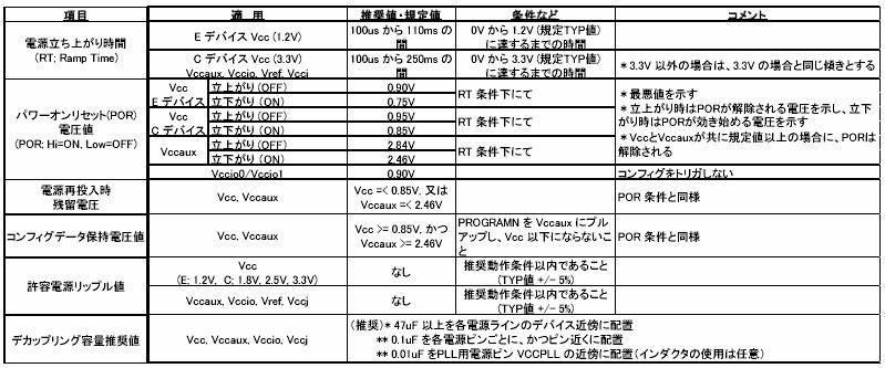
 Lattice FPGA 実装設計と ボード設計の ガイドライン 本ドキュメントは主にラティス代理店 FAE を対象としています - 1 - 目次 1 はじめに 5 2 Lattice FPGA 各ファミリの電源設計要件 6 2.1 LatticeECP3 ファミリ... 6 2.1.1 電源系統と推奨電圧範囲... 6 2.1.2 電源のランプレート ( 傾き ) 立ち上がり時間... 6 2.1.3
エンハンスド・コンフィギュレーション・デバイス(EPC4、EPC8 & EPC16)データシート
データシート") 2. EPC4 EPC8 & EPC16 CF52002-2.2 EPC4 EPC8 EPC16 Stratix Cyclone APEX II APEX 20K APEX 20K APEX 20KC APEX 20KE Mercury ACEX 1K FLEX 10KFLEX 10KE FLEX 10KA 4 8 16 / EPC16 EPC4 8 Stratix FPP DCLK 8 FPGA
2. EPC4 EPC8 & EPC16 CF52002-2.2 EPC4 EPC8 EPC16 Stratix Cyclone APEX II APEX 20K APEX 20K APEX 20KC APEX 20KE Mercury ACEX 1K FLEX 10KFLEX 10KE FLEX 10KA 4 8 16 / EPC16 EPC4 8 Stratix FPP DCLK 8 FPGA
c3 FAST RETAILING ANNUAL REPORT 2006
 c3 FAST RETAILING ANNUAL REPORT 2006 FAST RETAILING ANNUAL REPORT 2006 c4 2 FAST RETAILING ANNUAL REPORT 2006 FAST RETAILING ANNUAL REPORT 2006 3 4 FAST RETAILING ANNUAL REPORT 2006 FAST RETAILING ANNUAL
Cyclone II Device Handbook
 VI. Cyclone II Cyclone II JTAG 13 Cyclone II 14 Cyclone II IEEE 1149.1 (JTAG) Altera Corporation VI 1 Preliminary Cyclone II, Volume 1 13 14 / 13 2004 11 v1.1 2004 6 v1.0 14 2004 6 v1.0 AS AS 13-8 MAX
 t-co 2 4000 3500 3000 2500 2000 1500 1000 500 0 167 128 116 191 239 183 88 96 87 360 369 360 68 78 3638 64 3676 3509 7 8 8 14 12 10 8 11 3 6 6 6 4 4 3 4 7 7 2 5 1 1 2 1 2 1 1 2 0 0 0 650 638 627

R1EV5801MBシリーズ データシート
 1M EEPROM (128-kword 8-bit) Ready/Busy and function R10DS0209JJ0100 Rev.1.00 131072 8 EEPROM ROM MONOS CMOS 128 2.7V 5.5V 150ns (max) @ Vcc=4.5V 5.5V 250ns(max) @ Vcc=2.7V 5.5V 20mW/MHz (typ) 110µW (max)
oaks32r_m32102
 OAKS32R-M32102S6FP 2 OAKS32R OAKS32R-M32102S6FP M32102S6FP... 4... 5... 6... 7 4.1. CPU...7 4.2. Flash ROM SDRAM....8 4.3. LANC....8 4.4. RS232C....9 4.5. CPU....9 4.6.....9 4.7....10 4.8. SDI....10...
R1RW0408D シリーズ
 お客様各位 カタログ等資料中の旧社名の扱いについて 2010 年 4 月 1 日を以って NEC エレクトロニクス株式会社及び株式会社ルネサステクノロジが合併し 両社の全ての事業が当社に承継されております 従いまして 本資料中には旧社名での表記が残っておりますが 当社の資料として有効ですので ご理解の程宜しくお願い申し上げます ルネサスエレクトロニクスホームページ (http://www.renesas.com)
N12866N2P-H.PDF
 16Mx64bits PC133 SDRAM SO DIMM Based on 16Mx16 SDRAM with LVTTL, 4 banks & 8K Refresh (16M x 16bit) /. / 1 A0 ~ A12 BA0, BA1 CK0, CK1 CKE0 /S0 /RAS /CAS /WE DQM0 ~ DQM7 DQ0 ~ DQ63 SA0~2 SDA SCL VCC 3.3
ネットリストおよびフィジカル・シンセシスの最適化
 11. QII52007-7.1.0 Quartus II Quartus II atom atom Electronic Design Interchange Format (.edf) Verilog Quartus (.vqm) Quartus II Quartus II Quartus II Quartus II 1 Quartus II Quartus II 11 3 11 12 Altera
Quartus II はじめてガイド ‐ Device and Pin Options 設定方法
 ALTIMA Corp. Quartus II はじめてガイド Device and Pin Options 設定方法 ver.10.0 2010 年 9 月 ELSENA,Inc. Quartus II はじめてガイド Device and Pin Options 設定方法 目次 1. はじめに... 3 2. Device and Pin Options の起動... 3 3. Device and
Arduino UNO IS Report No. Report Medical Information System Laboratory
 Arduino UNO 2015 2 25 IS Report No. Report Medical Information System Laboratory Abstract ( ) Arduino / Arduino Bluetooth Bluetooth : Arduino Arduino UNO Arduino IDE micro computer LED 1............................
Quartus Prime はじめてガイド - デバイス・オプションの設定方法
 ALTIMA Corp. Quartus Prime はじめてガイドデバイス オプションの設定方法 ver.15.1 2016 年 5 月 Rev.3 ELSENA,Inc. Quartus Prime はじめてガイド デバイス オプションの設定方法 目次 1. 2. はじめに...3 デバイス オプションの設定...4 2-1. 2-2. 2-3. 2-4. 2-5. 2-6. 2-7. 2-8.
Unidirectional Measurement Current-Shunt Monitor with Dual Comparators (Rev. B
 www.tij.co.jp INA206 INA207 INA208 INA206-INA208 INA206-INA208 V S 1 14 V IN+ V S 1 10 V IN+ OUT CMP1 IN /0.6V REF 2 3 1.2V REF 13 12 V IN 1.2V REF OUT OUT CMP1 IN+ 2 3 9 8 V IN CMP1 OUT CMP1 IN+ 4 11
untitled
 AWG-50 Rev 6.5 1 4 2 5 3 5 4 6 4.1 6 4.2 6 4.3 7 4.4 7 4.5 8 4.6 8 4.7 8 4.8 9 5 CD-ROM 10 6 11 6.1 11 6.1.1 Windows 10 11 6.1.2 Windows 8 8.1 12 6.1.3 Windows 7 13 6.1.4 Windows Vista 14 6.1.5 Windows
イントロ
 AWA BANK REPORT 2014 AWA BANK REPORT 2014 AWA BANK REPORT 2014 P15 P16 P17 P19 P18 P18 P17 AWA BANK REPORT 2014 0120-167-925 CLOSE UP CLOSE UP AWA BANK REPORT 2014 117 AWA BANK REPORT 2014 0120-888-522
untitled
 TC78S6FTG TC78S6FTG TC78S6FTG 2 PWM 1-2 W1-2 2W1-24W1-2 (1) V CC 2.7~5.5 6 V VM 2.5~15 18 V : (2) / STBY = Low ENABLE = Low STBY = High ENABLE = High 1. 1. A (peak) 1 TC78S6FTG 2. PD-Ta Ta 85 Power dissipation
B1 Ver ( ), SPICE.,,,,. * : student : jikken. [ ] ( TarouOsaka). (, ) 1 SPICE ( SPICE. *1 OrCAD
![B1 Ver ( ), SPICE.,,,,. * : student : jikken. [ ] ( TarouOsaka). (, ) 1 SPICE ( SPICE. *1 OrCAD](/thumbs/101/152175529.jpg "B1 Ver ( ), SPICE.,,,,. * : student : jikken. [ ] ( TarouOsaka). (, ) 1 SPICE ( SPICE. *1 OrCAD") B1 er. 3.05 (2019.03.27), SPICE.,,,,. * 1 1. 1. 1 1.. 2. : student : jikken. [ ] ( TarouOsaka). (, ) 1 SPICE ( SPICE. *1 OrCAD https://www.orcad.com/jp/resources/orcad-downloads.. 1 2. SPICE 1. SPICE Windows
B1 er. 3.05 (2019.03.27), SPICE.,,,,. * 1 1. 1. 1 1.. 2. : student : jikken. [ ] ( TarouOsaka). (, ) 1 SPICE ( SPICE. *1 OrCAD https://www.orcad.com/jp/resources/orcad-downloads.. 1 2. SPICE 1. SPICE Windows
Triple 2:1 High-Speed Video Multiplexer (Rev. C
 www.tij.co.jp OPA3875 µ ± +5V µ RGB Channel OPA3875 OPA3875 (Patented) RGB Out SELECT ENABLE RED OUT GREEN OUT BLUE OUT 1 R G B RGB Channel 1 R1 G1 B1 X 1 Off Off Off 5V Channel Select EN OPA875 OPA4872
(6) (111) (148) (129) (169) CAPCOM ANNUAL REPORT
 (111) (148) (129) (169) CAPCOM ANNUAL REPORT") 62 63 65 69 71 72 73 74 91 61 CAPCOM ANNUAL REPORT 213 22 26 276 143 92 13 113 73 122 (6) (111) (148) (129) (169) 23 24 25 27 28 29 21 211 212 213 CAPCOM ANNUAL REPORT 213 62 63 CAPCOM ANNUAL REPORT 213
62 63 65 69 71 72 73 74 91 61 CAPCOM ANNUAL REPORT 213 22 26 276 143 92 13 113 73 122 (6) (111) (148) (129) (169) 23 24 25 27 28 29 21 211 212 213 CAPCOM ANNUAL REPORT 213 62 63 CAPCOM ANNUAL REPORT 213
USB-Blasterダウンロード・ケーブル・ユーザガイド
 USB-Blaster 101 Innovation Drive San Jose, CA 95134 www.altera.com 2.3 2007 5 UG-USB81204-2.3 P25-10325-03 Copyright 2007 Altera Corporation. All rights reserved. Altera, The Programmable Solutions Company,
VLSI工学
 2008//5/ () 2008//5/ () 2 () http://ssc.pe.titech.ac.jp 2008//5/ () 3!! A (WCDMA/GSM) DD DoCoMo 905iP905i 2008//5/ () 4 minisd P900i SemiConsult SDRAM, MPEG4 UIMIrDA LCD/ AF ADC/DAC IC CCD C-CPUA-CPU DSPSRAM
Stratix IIIデバイスの外部メモリ・インタフェース
 8. Stratix III SIII51008-1.1 Stratix III I/O R3 SRAM R2 SRAM R SRAM RII+ SRAM RII SRAM RLRAM II 400 MHz R Stratix III I/O On-Chip Termination OCT / HR 4 36 R ouble ata RateStratix III FPGA Stratix III
How to read the marks and remarks used in this parts book. Section 1 : Explanation of Code Use In MRK Column OO : Interchangeable between the new part
 Reservdelskatalog MIKASA MVB-85 rullvibrator EPOX Maskin AB Postadress Besöksadress Telefon Fax e-post Hemsida Version Box 6060 Landsvägen 1 08-754 71 60 08-754 81 00 info@epox.se www.epox.se 1,0 192 06
How to read the marks and remarks used in this parts book. Section 1 : Explanation of Code Use In MRK Column OO : Interchangeable between the new part
 Reservdelskatalog MIKASA MT65H vibratorstamp EPOX Maskin AB Postadress Besöksadress Telefon Fax e-post Hemsida Version Box 6060 Landsvägen 1 08-754 71 60 08-754 81 00 info@epox.se www.epox.se 1,0 192 06
How to read the marks and remarks used in this parts book. Section 1 : Explanation of Code Use In MRK Column OO : Interchangeable between the new part
 Reservdelskatalog MIKASA MVC-50 vibratorplatta EPOX Maskin AB Postadress Besöksadress Telefon Fax e-post Hemsida Version Box 6060 Landsvägen 1 08-754 71 60 08-754 81 00 info@epox.se www.epox.se 1,0 192
1 1 2 2 2-1 2 2-2 4 2-3 11 2-4 12 2-5 14 3 16 3-1 16 3-2 18 3-3 22 4 35 4-1 VHDL 35 4-2 VHDL 37 4-3 VHDL 37 4-3-1 37 4-3-2 42 i
 1030195 15 2 10 1 1 2 2 2-1 2 2-2 4 2-3 11 2-4 12 2-5 14 3 16 3-1 16 3-2 18 3-3 22 4 35 4-1 VHDL 35 4-2 VHDL 37 4-3 VHDL 37 4-3-1 37 4-3-2 42 i 4-3-3 47 5 52 53 54 55 ii 1 VHDL IC VHDL 5 2 3 IC 4 5 1 2
EVBUM2170JP - LC87F1M16A評価ボードユーザーマニュアル
 EVAL BOARD USER S MANUAL Table 1. LC87F1M16A Version 0x1000 _Application.exe _driver.inf (USB DG1 1Ma1 EVK) USB-mini (FSS 43085 05 ) CD-ROM* 1 1 1 1 OS Windows XP profile.net Framework4 Client Profile
main.dvi
 CAD 2001 12 1 1, Verilog-HDL, Verilog-HDL. Verilog-HDL,, FPGA,, HDL,. 1.1, 1. (a) (b) (c) FPGA (d). 2. 10,, Verilog-HDL, FPGA,. 1.2,,,, html. % netscape ref0177/html/index.html.,, View Encoding Japanese
オンボード・フラッシュ・プログラマ FP-10技術資料
 2019-02-28 本資料は以下の内容で構成されています オンボード フラッシュ プログラマ FP-10 技術資料 ( 第 13 版 ) FP-10 を使用する前に参照していただく資料です FP-10 ユーザーズ マニュアル ( 第 59 版 ) - 抜粋版 ( ) FP-10 側ターゲット インターフェース仕様について記載されています FP-10 ユーザーズ マニュアルより 第 7 章ターゲット
NL-20取扱説明書_操作編
 MIC / Preamp A C AMP 1 AMP 2 AMP 3 FLAT FLAT CAL.SIG. OVER LOAD DET. AMP 4 AMP 5 A/D D/A CONV. V ref. AMP 8 AMP 10 DC OUT AC OUT AC DC OUT DATA BUS CPU ADDRESS BUS DSP Start Pause Stop Store Mode Cont
How to read the marks and remarks used in this parts book. Section 1 : Explanation of Code Use In MRK Column OO : Interchangeable between the new part
 Reservdelskatalog MIKASA MCD-L14 asfalt- och betongsåg EPOX Maskin AB Postadress Besöksadress Telefon Fax e-post Hemsida Version Box 6060 Landsvägen 1 08-754 71 60 08-754 81 00 info@epox.se www.epox.se
『赤すぐ』『妊すぐ』<出産・育児トレンド調査2003>
 79.9 1.6 UP 86.6% 7.0 UP 61.3% 12.7UP 18-24 3 66.6 3.0 UP 38.7 0.7 UP 14.8 1.9 UP 13.3 0.3UP 4 1 024 1.23 0.01down Topics 5 79.9 1.6UP 7.0 UP 12.7U 3.5 0.4 UP 3.4 0.4 UP 6 73.1% 5.7 UP 75.0% 71.2% 7 53.9%
pin-csp011.xls
 CSP-011-130E(EPF10K130ERC240) ピン番号 デバイスピン名称 信号名 内容 処理 1 TCK TCK JTAG:TCK プルダウン / 内部使用 2 CONF_DONE CONF_DONE CONF_DONE プルアップ / 内部使用 3 nceo nceo CEO プルアップ / 内部使用 4 TDO TDO JTAG:TDO プルアップ / 内部使用 5 VCCINT


LM2831 高周波数動作 1.5A 負荷 降圧型DC/DCレギュレータ
 High Frequency 1.5A Load - Step-Down DC-DC Regulator Literature Number: JAJSAH7 1.5A DC/DC 5 SOT23 6 LLP PWM DC/DC DC/DC PCB 0.5 m BiCMOS 1.5A 130m PMOS 30ns 3V 5.5V 0.6V 550 khz 1.6MHz 3.0MHz 93% 30nA
102
 5 102 5 103 q w 104 e r t y 5 u 105 q w e r t y u i 106 o!0 io!1 io q w e r t y 5 u 107 i o 108 q w e q w e r 5 109 q w 110 e r t 5 y 111 q w e r t y u 112 i q w e r 5 113 q w e 114 r t 5 115 q w e 116
TULを用いたVisual ScalerとTDCの開発
 TUL を用いた Visual Scaler と TDC の開発 2009/3/23 原子核物理 4 年 永尾翔 目次 目的と内容 開発環境 J-Lab におけるハイパー核分光 Visual Scaler TDC まとめ & 今後 目的と内容 目的 TUL, QuartusⅡ を用いて実験におけるトリガーを組めるようになる Digital Logic を組んでみる 内容 特徴 TUL,QuartusⅡ
電源監視回路
 TPS3820-xx,TPS3823-xx TPS3824-xx,TPS3825-xx TPS3828-xx www.tij.co.jp µ TYPICAL APPLICATION TPS3820, TPS3823, TPS3828: DBV PACKAGE (TOP VIEW) GND MR 1 2 3 5 4 VDD WDI TPS3824: DBV PACKAGE (TOP VIEW) 1 5