スライド 1
|
|
|
- なごみ しどり
- 5 years ago
- Views:
Transcription
1 WG13 Emerging Research Materials (ERM) イノベーションエンジンとしての ERM 秋永広幸 ( 産総研 : リーダー ) 酒井忠司 ( 東芝 : サブリーダー ) 佐藤信太郎 ( 産総研 : 幹事 ) 青井信雄 ( パナソニック ) 粟野祐二 ( 慶應大 ) 内田健 ( 東工大 ) 大野雄高 ( 名大 ) 大森克実 (TOK) 苅谷隆 ( イビデン ) 佐々木秀幸 ( 東芝ナノアナリシス ) 品田賢宏 ( 早大 ) 杉山直之 ( 東レリサーチ ) 関谷瑞木 ( 産総研 ) 戸所義博 ( 奈良先端大 ) 富岡泰秀 ( 産総研 ) 野田啓 ( 京大 ) 松倉文礼 ( 東北大 ) 松澤伸行 ( ソニー ) 宮本良之 ( 産総研 ) 由上二郎 ( ルネサスエレ ) 和田恭雄 ( 東洋大 ) 1
2 用語集 CNT Carbon Nanotube CTE Coefficient of thermal expansion DSA Directed Self Assembly ERD Emerging Research Device (WG) ERM Emerging Research Material (WG) ESH Environment, Safety and Health EUV Extreme Ultra-Violet FEFET Ferroelectric Field Effect Transistor FEP Front End Process (WG) GNR Graphene Nano Ribbon ILD Inter Layer Dielectrics NEMS Nano Electro Mechanical Systems PIDS Process Integration, Devices, and Structures SAM Self-Assembled Monolayer STT Spin-Transfer Torque 2
3 ERM のミッション ミッション : 各 ITWG の抱える 困難な技術課題 を解決する可能性のある ERM について その技術的 時間的要請を明らかにすること 取り組み : 1) 各 ITWG のニーズを明らかにする 2) ニーズを満たす可能性のある ERM 候補を探し出す 3) ニーズとの技術的ギャップを明らかにする 複数候補がある場合 それらを比較検討する 4) 実現すべき時期を明らかにする 3
4 ERM のスコープ ERD 材料 (Memory 用材料 Logic 用材料 ) 低次元材料 (Low Dimensional Materials: ナノ微粒子 ナノワイヤ CNT ク ラフェン他 ) 界面 & ヘテロ界面 スピン材料 (Spin Materials) 複合金属酸化物 (Complex Metal Oxides) 機能性 ( 巨大 ) 分子 (Macromolecules) 制御された自己組織化材料 (Directed self-assemble) リソグラフィ材料 (Directed self-assemble 材料を含む ) FEP Interconnect ASP 材料 確定的ドーピング (Deterministic doping) ESH (Environment, Safety, and Health) 計測 (Metrology) シミュレーション (Simulation) その他 4
5 ERM のスコープ 材料 ERD メモリ ERD ロジックリソグラフィ フロントエンドプロセス 配線 アッセンブリ & パッケージング 低次元材料 NEMS メモリ ナノチューブナノワイヤグラフェン他炭素材料 High-index Immersion liquid ナノチューブ金属ナノワイヤ 電気的応用熱応用機械的応用 機能性分子 ( 巨大分子 ) 分子メモリ 分子デバイス レジストインプリント用ポリマー 新規洗浄選択エッチンク 選択デポ 低誘電率 ILD ホ リマーの電気的 熱的 機械的性能制御 自己組織化材料 リソク ラフィ内ハ ターン形成 超高精度寸法制御 選択エッチンク 選択デポ確定的ドーピング 選択エッチンク 選択デポ 高性能キャパシタ スピン材料 STT-RAM スヒ ン依存伝導強磁性半導体トンネル絶縁体 複合金属酸化物 ( 遷移金属酸化物 ) 1Tr-FeRAM Redox RAM マルチフェロイック材料新規相転移 高性能キャパシタ 接合とヘテロ界面 電気的 スヒ ン伝導の電極と接合界面 電気的 スヒ ン伝導の電極と接合界面 電極と接合界面 5
6 ERM の国内メンバー Sharing roles Members Introduction (Scope, etc) 全員 (20 名 ) Emerging Research Device Material 粟野 ( 慶大 ) 酒井 ( 東芝 ) 内田 ( 東工大 ) 大野 ( 名大 ) 佐藤 ( 産総研 ) 和田 ( 東洋大 ) 松澤 ( ソニー ) 野田 ( 京大 ) 松倉 ( 東北大 ) 富岡 ( 産総研 ) 杉山 ( 東レリサーチ ) 秋永 ( 産総研 ) Lithography Materials 戸所 ( 奈良先端大 ) 由上 ( ルネサスエレ ) 大森 (TOK) 品田 ( 早大 ) Emerging FEP and PIDS Materials 由上 ( ルネサスエレ ) Interconnects 青井 ( ハ ナソニック ) 粟野 ( 慶大 ) 酒井 ( 東芝 ) 佐藤 ( 産総研 ) Assembly and Package 苅谷 ( イビデン ) 佐藤 ( 産総研 ) 大野 ( 名大 ) Environment, Safety, and Health Metrology 関谷 ( 産総研 ) 佐々木 ( 東芝ナノアナリシス ) Modeling and Simulation 宮本 ( 産総研 ) 現在 21 名 ナノエレ全般に対応できる国内有数の専門家集団に成長 杉山 ( 東レリサーチ ) 6
7 ERM の国際メンバー STRJ メンバー取りまとめ役 Hiro Akinaga, Jesus de Alamo, Dimitri Antoniadis, Nobuo Aoi, Masakazu Aono, Koyu Asai, Asen Asenov, Yuji Awano, David Awschalom, Rama Ayothi, Kaustav Banerjee, Chris Bencher, Agnès Barthélémy, Daniel-Camille Bensahel, Kris Bertness, Stacey Bent, Mikael Björk, August Bosse, Bill Bottoms, George Bourianoff, Rod Bowman, Alex Bratkovski, Robert Bristol, Ahmed Busnaina, Jeff Calvert, John Carruthers, Bernie Capraro, Chris Case, David Chan, An Chen, Eugene Chen, Zhihong Chen, Joy, Cheng, Toyohiro Chikyow, Byung Jin Cho, U-In Chung, Jonathan Coleman, Luigi Colombo, Johann Coraux, Hongjie Dai, Ralph Dammel, Juan DePablo, Anton Devilliers, Thibaut Devolder, B. Dieny, Jean Dijon, Athanasios Dimoulas, Catherine Dubourdieu, John Ekerdt, Tetsuo Endoh, James Engstrom, Thomas Ernst, Michael Flatte, Glenn Fredrickson, Gregory Fuchs, Satoshi Fujimura, C. Michael Garner, Emmanuel Giannelis, Niti Goel, Michael Goldstein, Suresh Golwalkar, Guido Groeseneken, Roel Gronheid, Wilfried Haensch, Cliff Henderson, Daniel Herr, Hiro Hibino, Marc Hillmyer, Bill Hinsberg, Toshiro Hiramoto, Judy Hoyt, Greg Hughes, Jim Hutchby, Harold Hwang, Hyunsang Hwang, K. Inoue, Takamasa Ishigaki, Saori Ishizu, Nobuyuki Ishiwata, Yoshio Ishiwata, Kohei Ito, Taisuke Iwai, Ajey Jacob, Raj Jami, David Jamieson, Ali Javey, James Jewett, Berry Jonker, Xavier Joyeux, Yeon Sik Jung, Ted Kamins, Zia Karim, Takashi Kariya, Masashi Kawaski, Leo Kenny, Richard Klein, Philip Kim, Sang Ouk Kim, Michael Kozicki, Mark Kryder, Roger Lake, Steve Lange, Sean King, Atsuhiro Kinoshita, Gabriel Kotliar, Victor Krivokapic, Mark Kryder, Yi-Sha Ku, Hiroshi Kumigashira, Nabil Laachi, Jang Ein Lee, Yi Jun Lee, Harry Levinson, Chenhsin Lien, Liew Yun Fook, Lloyd Litt, Scott List, Chi Chun Liu, Wei-Chung Lo, Louis Lome, Gerry Lucovsky, Mark Lundstrom, Yale Ma, Allan MacDonald, Blanka Magyari-Kope, Prashant Majhi, Arun Majumdar, Francois Martin, Lane Martin, Witek Maszara, Jennifer McKenna, Fumihiro Matsukura, Nobuyuki Matsuzawa, Claudia Mewes, Dan Millward, Yoshiyuki Miyamoto, Stephane Monfray, Andrea Morello, Mick Morris, Azad Naeemi, Boris Naydenov, C Gomez-Navarro, Paul Nealey, Kwok Ng, Fumiyuki Nihey, Mizuhisa Nihey, Yoshio Nishi, Kei Noda, Yaw Obeng, Chris Ober, Katsumi Ohmori, Yutaka Ohno, Laurent Pain, Ray Pearson, Jeff Peterson, Er-Xuan Ping, Alexei Preobrajenski, Victor Pushparaj, Ganapati Ramanath, Ramamoorthy Ramesh, Nachiket Raravikar, Ben Rathsack, Curt Richter, Heike Riel, Dave Roberts, Sven Rogge, Jae Sung Roh, Ricardo Ruiz, Thomas Russell, Tadashi Sakai, Gurtej Sandhu, Krishna Saraswat, Hideyuki Sasaki, Mitusru Sato, Shintaro Sato, Barry Schechtman, Thomas Schenkel, Jan Seidel, Mizuki Sekiya, Sadasivan Shankar, Matthew Shaw, Takahiro Shinada, Michelle Simmons, K. Singer, Kaushal K. Singh, Jon Slaughter, Mark Slezak, Bruce Smith, Tom Smith, Mark Somervell, Mark Stiles, Tsung-Tsan Su, Maki Suemitsu, Naoyuki Sugiyama, Chun-Yung Sung, Raja Swaminathan, Michiharu Tabe, Hidenori Takagi, Shin-ichi Takagi, Koki Tamura, Shinji Tarutani, Raluca Tiron, Yoshihiro Todokoro, Yasuhide Tomioka, Peter Trefonas, Ming-Jinn Tsai, Wilman Tsai, Vincent Tung, King Tu, Mark Tuominen, Ken Uchida, Marc Ulrich, Philippe Vereecken, Yasuo Wada, Vijay Wakharkar, Kang Wang, Weie Wang, Zhong Lin Wang, Rainer Waser, Jeff Welser, Lars-Erik Wernersson, Andrew Whittaker, Grant Willson, C.P. Wong, H.S. Philip Wong, Dirk Wouters, Wen-Li Wu, Hiroshi Yamaguchi, Toru Yamaguchi, Chin-Tien Yang, Kenji Yoshimoto, Yi-Sha Yu, SC Zhang, Yuegang Zhang, Jiro Yugami, Victor Zhirnov, Paul Zimmerman, Chuck Zmanda 7
8 Table ERM1 Emerging Research Material Technologies Difficult Challenge ( ) Difficult Challenges Achieving desired properties in integrated structures Chareacterize and control coupled properties of embedded materials and their interfaces Identifying manufacturable methodologies to enable deterministic fabrication with required property control Ability to control defects in material processing Control of Self-assembly processes to achieve desired properties reproducibly Summary of Issues Achieving high hole mobility in III-V materials Achieving high electron mobility in Ge with low contact resistivity Wafer scale growth of high quality graphene with desired process conditions (ex. Low temperature growth on metal or insulator) Achieving a bandgap in graphene Synthesis of CNTs with controlled diameters, chirality and site-density Multiferroic with Curie temperature >400K and high remnant magnetization to >400K Ferromagnetic semiconductor with Curie temperature >400K Wafer scale growth of high quality graphene with desired process conditions (ex. Low temperature growth on metal or insulator) Synthesis of CNTs with controlled diameters and site-density Electric control of the electron correlation, ex. Mott transition, Spin dynamics High hole mobility in III-V materials with unpinned Fermi level and ohmic contact High electron mobility in Ge with unpinned Fermi level and ohmic contact High mobility in nanowires with unpinned Fermi level Graphene with a bandgap, high mobility, and unpinned Fermi level at dielectric interfaces Complex metal oxides with unpinned Fermi levels Electric control of oxygen vacancies, ex. the distribution and the charged state Nanoscale observation of the magnetic domain structure, for example, the domain in STT-RAM under the magnetic field, i.e., the dynamic operation Characterization of electrical properties of molecule / metal contact interfaces (i.e. Pentacene/Au) Characterization of electrical properties of embedded nano contact interfaces (i.e. CNT/Metal ) Characterization for density of dislocations and anti-phase boundary generating interface between Ge/III-V channel materials and Si Dopant placement and activation i.e. deterministic doping with desired number at precise location for Vth control and S/D formation in Si as well as alternate materials HVM compatible methods to place dopants in predetermined positions with minimal damage to the semiconductor Controlled fabrication of nanostructured materials and devices (ex. Graphene nanoribbon, graphene nanomesh) Controlling edge-termination / molecular absorption to graphene to achieve required bandgap Methods to place carbon nanotubes in predetermined locations Assembly of CNTs or graphene into predetermined arrays and locations HVM methods to deposit graphene on dielectric surfaces Methods to reduce directed self assembly based defects to <0.01cm-2 for litho extension Control defects in carbon nanotubes Control defects in growth and processing of graphene Control concentration and locations of cation and anion defects in complex metal oxides Control precipitation in ferromagnetic semiconductors Characterization for density of dislocations and anti-phase boundary generating interface between Ge/III-V channel materials and Si Simultaneously achieve required feature sizes in predetermined arrays with low anneal time, low defect density Registration of self-assembled patterning materials in desired locations with control of geometry, conformation, interface roughness, and defects DSA application to the realistic device pattern with reduced pattern roughness and defects Decrease of DSA patterning process time 8
9 Table ERM1 Emerging Research Material Technologies Difficult Challenge ( ) Difficult Challenges Electric field control of the electrochemcal reaction in a nanoscaled device and at an interface Metrology to characterize structure and properties of materials at the nanometer scale Summary of Issues Complex Oxides: Control of oxygen vacancy formation at metal interfaces and interactions of electrodes with oxygen and vacancies Switching mechanism of atomic switch. Improvements in switching speed, cyclic endurance, uniformity of the switching bias voltage and resistances both for the on-state and the off-state. Nano-Carbon / metal functinal junction, such as new switch, by using electrochemical reactions Molecular device fabrication with precise control using electrochemical reactions III-V: Correlation between antiphase domains and electrical properties Development of the method to evaluate the validity of the measurement result for each ERM Electrical and thermal properties of each carbon nanotube Nanowire characterization of mobility, carrier density, interface states, and dielectric fixed charge effects Graphene mobility and carrier concentration Complex metal oxide characterization of carrier density, dielectric and magnetic properties Spin materials: characterization of spin, magnetic and electrical properties and correlation to nanostructure Metrology to characterize defects at the nanometer scale with atomic resoiution Characterization of electrical properties of embedded nano contact interfaces (ex. CNT/Metal ) Evaluating material properties in realistic device structures Nanoscale observation of the magnetic domain structure, for example, the domain in STT-RAM under the magnetic field, i.e., the dynamic operation Antiphase domains within III-V semiconductors and their interfaces with high κ dielectrics CNT vacancy and interstitial ordering around dopants Nanowires: Characterization of vacancies, interstitials and dopants within the NW and at interrfaces to dielectrics Graphene: Characterization of edge defects, vacancies and interstitials within the material and at interfaces Metal nanoparticles: Native oxide interface and crystal defects in the nanoparticle Complex Oxides: Location of oxygen vacancies and the valence of the metal ions Spin materials: characterization of vacancies in spin tunnel barriers, and defects within magnetic materials and at their interfaces Accurate multiscale simulation for predictions of unit processes the resulting structure, properties and device performance. Evaluating material properties IN realistic nm scale devices Characterization of edge structure and termination with atomic resolution (ex. Graphene nano ribbon ) Linkage between different scales in time, space, and energy bridging non-equilibrium phenomena to equilibrium phenomena Transferable simulation tools for many kinds of materials Development of platform for different simulation tools, such as TCAD and ab-initio calculations Nanowires: Simulation of growth and defect formation within and at interfaces CNTs: Simulation of growth and correlation to bandagap Graphene: Simulation of synthesis, edge defects, vacancies, interstitials, interfacial bonding, and substrate interactions. Nanoparticles: Simulation of growth and correlation to structure and defects Complex Oxides: Multiscale simulation of vacancy fomation, effect on metal ion valence state and effect of the space charge layer Spin: Improved models for multiscale simulation of spin properties within materials and at their interfaces. Fundamental thermodynamic stability and fluctuations of materials and structures Geometry, conformation, and interface roughness in molecular and self-assembled structures Device structure-related properties, such as ferromagnetic spin and defects Dopant location and device variability 9
10 ERM の挑戦的課題 (2011~2018) 1, 集積化された構造において所望の機能を発現させること III-V 族半導体 Ge 半導体における高い移動度 ウェハ寸法で良質のグラフェンを形成すること 400K 以上の強磁性転移温度を持つ磁性半導体 電子相関 ( モット転移等 ) の電界制御 2, 埋め込まれた構造や界面にて複合機能の評価と制御を行うこと III-V 半導体 Ge 半導体におけるフェルミレベル ( ピニング ) の制御 CNT / 金属界面 分子 / 金属界面におけるコンタクト抵抗の制御 酸化物材料における酸素欠陥分布とその荷電状態の電界制御 3, 所望の特性を引き出す確定的 ( 決定論的 ) 製造技術を開発する方法論を確立すること High-volume manufacturing (HVM) に適用可能で 低ダメージの確定論的ドーピング技術 位置と個数を精密に定める確定論的ドーピング技術を用いた Vth と S/D の制御 端面終端や分子吸着によるグラフェンの特性制御 4, 材料合成の過程で欠陥を制御すること DSA リソ材料における欠陥密度の低減 (10nm 以上の Defect 密度が <0.01 個 /cm 2 ) 酸化物材料におけるカチオン アニオン欠陥の制御 強磁性半導体における偏析制御 III-V 族半導体 Ge 半導体チャネルにおける界面での転移や逆位相境界密度の低減 5, 所望の特性を再現性高く実現する自己組織化現象を制御すること 幾何的形状 形態 界面粗さ 欠陥を制御した材料の自己組織化による精密配置 10
11 ERM の挑戦的課題 (2019~2026) 6, ナノデバイスや界面における固体化学的反応の精密な電界制御を可能とすること 酸化物材料と金属界面における欠陥と界面反応の電界制御 原子スイッチの速度 買換回数 信頼性と抵抗値の高性能化 固体化学的手法を用いたナノサイズ分子デバイスの形成 7, ナノメートル領域における材料の構造と特性の評価 III-V 族半導体 : 逆位相境界と電気特性の相関 ナノワイヤーの移動度 キャリア濃度 界面欠陥密度 絶縁膜の固定電荷の影響の評価 CNT / 金属界面等 埋め込まれた界面における電気的特性の評価 ( ナノメートルサイズの ) 実デバイスにおける特性の評価 8, 原子レベル分解能での欠陥評価 グラフェンナノリボンにおける端面とその終端状態の原子レベル評価 微粒子における自然酸化膜界面や欠陥の評価 スピン材料 : トンネル絶縁膜内の欠陥 強磁性金属 / 絶縁膜界面の評価 CNT / 金属界面等 埋め込まれた界面における電気的特性の評価 9, 精密なマルチスケール計算による構造 物性 デバイス特性の予測 非平衡現象から平衡状態まで包括的にシミュレーションする為に 空間と時間 およびエネルギーの異なるスケールをつなぐこと 様々な材料に適用できるシミュレーションツールの開発 TCAD と第一原理計算など異なるシミュレーションツールの連結 10, 材料そのものの熱安定性と揺らぎの制御 分子材料 自己組織化材料における幾何的形状 形態 界面粗さの制御 11

 Copyright 2011 American Chemical Society.\" 担当 : 佐藤委員 新たなグラフェン転写法 (Reprinted with permission from Wang et al., VLSI Symp. Tech. Dig., p.1 16(2011).")
12 ナノカーボン材料 ( グラフェン ) ITRS2011 改訂内容と注目点 グラフェンの形成 形成法として 前回同様 機械的剥離 SiCの高温アニール CVD の3つが挙げられている SiC CVDの参考文献がアップデートされたが 機械的剥離法や酸化グラフェンを用いた手法の詳細は省略された CVDでグラフェンを形成した後 通常はグラフェンを転写するが 新たに転写をしない方法 新たな転写法にについて言及 グラフェンの移動度 サスペンデッドグラフェンの移動度は 240K で 120,000 cm2/vs 室温付近では Flexural phonon により移動度は減少する BN に挟まれた剥離グラフェンで 室温で 100,000 cm2/v 程度 SiC グラフェンでは 15,000 cm2/vs CVD では 16,000 cm2/vs 程度が室温で得られた BN/Graphene/BN デバイスとその電気特性 "Reprinted with permission from Mayorov et al., Nano lett. Vol.11, p.2396 (2011) Copyright 2011 American Chemical Society." 担当 : 佐藤委員 新たなグラフェン転写法 (Reprinted with permission from Wang et al., VLSI Symp. Tech. Dig., p.1 16(2011). Copyright 2011 JSAP 12


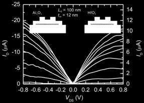
13 ナノカーボン材料 ( グラフェン ) ITRS2011 改訂内容と注目点 バンドギャップの形成 ナノリボン化 2 層グラフェンに電場を印加する方法に加え グラフェンに周期的な孔を開ける方法 基板 (SiC BN MgO) との相互作用を利用する方法などに言及 リボン化においては エッジの処理が重要な点を指摘 高誘電率膜の堆積 大きな進展は無いが High-k 膜を Low-k バッファ層を介して ALD 堆積する方法を紹介 バッファ層を介して HfO2 膜を堆積したグラフェントランジスタの特性 "Reprinted with permission from Farmer et al., Nano lett. Vol.9, p.4478 (2009) Copyright 2009 American Chemical Society." 担当 : 佐藤委員 グラフェンナノメッシュデバイス Reprinted by permission from Macmillan Publishers Ltd: Bai et al., Nature Nanotechnology. Vol.5, p.190 (2010), copyright 2010 ドーピング 大きなアップデートは無く 異種材料との接触による電荷移動によってドープする方法 エッジを修飾することによりドーピングする手法を紹介 ピリジンを原料ガスとして Nドープグラフェンを直接合成する方法が新たに言及された コンタクトの形成 コンタクト抵抗に関しいくつかの新たな文献を挙げているが コンタクト抵抗はまだ高い 13
14 ナノカーボン材料 (CNT) 担当 : 大野委員 CNT FET MATERIALS 改定内容 Bandgap Control 半導体 CNT 純度 : CVD 95%, 分離 99% 分離 CNT の場合 分散剤除去プロセスが必要 追加 純度評価技術の開発が必要 追加 Control of Position and Direction CVD: 20~50 aligned CNTs/μm 分離 CNT: ~20 aligned CNTs/μm 追加 Control of Carrier Concentration (Nanotube Doping) 大きな進展なし 新技術 :high k 膜界面電荷によるキャリア注入制御 Gate Dielectric Interface 分離技術に進展 主に分離 CNT 関連の記述を追加 新技術 : 濡れのよい金属 (Y, Ti) を酸化する方法 (Y 2 O 3 : 5 nm => EOT ~ 1 nm) Contact Formation 大きな進展はなし (pmos: Pd, nmos: Sc, Y) 新技術 : コンタクト付近の電位を high k 膜中電荷で変調し低抵抗化 14

 担当 :")


")

15 ナノカーボン材料 (CNT) Bandgap Control 高純度半導体 / 金属分離 ゲルクロマトグラフィ半導体 >99 % Nano Res. 4, 963 (2011) 担当 : 大野委員 Bandgap control and Control of position and direction Control of Position and Direction Langmuir-Blodgett 法による高密度配向 CNT ~50 CNTs/μm JACS 129, 4890 (2007) 単一カイラリティ分離 >99 %, (10,5) CNT 溶液プロセスによる自己整合 配向 CNT 膜 半導体 CNT, >20 CNTs/μm ACS Nano 2, 2445 (2008) JACS 131, 2454 (2009) 15


 担当 : 大野委員 and")


16 ナノカーボン材料 (CNT) Control of Carrier Pd 電極 -> p 型 ほぼ対称なpMOS, nmos 特性を実現 Sc 電極 -> n 型 極薄 high-k の均一成膜 Y 2 O 3 : 5 nm (EOT ~ 1 nm) 担当 : 大野委員 Control of Carrier and Formation of Gate Dielectric Formation of Gate Dielectric on graphene ゲート絶縁膜界面の固定電荷によるキャリア注入制御 APEX 3, (2010) Nano Lett. 10, 2024 (2010) 16
 磁壁移動素子スピン FET 磁気トンネル接合 (MTJ) を用いたスピントロニクス SPRAM (spin transfer torque RAM) 不揮発 高速")
 低スィッチング電流 (I C < F μa; F = feature size) 不揮発性のための高い熱安定性 (E/k B T > 40) CMOS BEOL に整合する高い熱耐性 (T a")
17 スピントロニクス材料 担当 : 松倉委員 スピントロニクス材料強磁性体材料 ( 不揮発 高スピン偏極 スピン注入 検出電極 ) 障壁材料 ( スピン フィルタリング ) チャネル材料 ( スピン緩和 スピン輸送 ) スピントロニクス素子磁気トンネル接合 (TMR STT ダイオード ) 磁壁移動素子スピン FET 磁気トンネル接合 (MTJ) を用いたスピントロニクス SPRAM (spin transfer torque RAM) 不揮発 高速 高書き換え耐性ロジック - イン - メモリ構成 静的消費電力の低減 配線遅延の低減 ITRS2011 は 2009 から大幅な変更は無し Memory Processor core MTJ CMOS 垂直磁気異方性 CoFeB/MgO/CoFeB MTJ 技術的課題 高出力 (TMR 比 > 100%) 低スィッチング電流 (I C < F μa; F = feature size) 不揮発性のための高い熱安定性 (E/k B T > 40) CMOS BEOL に整合する高い熱耐性 (T a > 350 o C; T a : 熱処理温度 ) 17
 が期待される 垂直磁気異方性 Mn 3-δ Ga 合金 CoFe/MgO MTJ V pulse = 1.5 V (0.55 ns) α, Innovation Engine! K, 2011 年 3 月 23 日東北大学プレスリリースより S.")
 2011 年 11 月 11 日大阪大学プレスリリースより Y. Shiota et al., Nature Mater. 11, 39 (2012). http://www.")
18 スピントロニクス材料 高磁気異方性 K + 低ダンピング α 熱安定指数 : Δ K スイッチング電流 : I C0 αk 高 Δ & 低 I C0 高 K & 低 α 材料が必要 担当 : 松倉委員 電圧印加磁化反転不揮発性素子で DRAM 並のスイッチング電力 (SPRAM の 1/1000 程度 ) が期待される 垂直磁気異方性 Mn 3-δ Ga 合金 CoFe/MgO MTJ V pulse = 1.5 V (0.55 ns) α, Innovation Engine! K, 2011 年 3 月 23 日東北大学プレスリリースより S. Mizukami et al., Phys. Rev. Lett. 106, (2011). TMR 比向上が課題 ( 現状で ~10% at RT) 2011 年 11 月 11 日大阪大学プレスリリースより Y. Shiota et al., Nature Mater. 11, 39 (2012). 18
19 酸化物材料 担当 : 富岡委員 4.4. Complex Metal Oxide Materials, interfaces and Superlattices A major challenge is to control the properties with an external field, for example, modulating and controlling conductivity with an electric field. 2011, Electric field control of the temperature for the Mott (metal insulator) transition. Tuning of the Mott (orbital ordering) transition in an electrolyte-gated FET structure with NdNiO 3 as a channel material Complex oxides for spintronics: Magnetic and magnetoresistive oxides Conducting ferromagnets, La 0.7 Sr 0.3 MnO 3, Sr 2 FeMoO 6 a conducting electrode in various devices for heteroepitaxy with other perovskites. for spintronics devices, such as magnetic tunnel junctions or spin filters. 2011, a heteroepitaxial perovskite metal-base (La 0.7 Sr 0.3 MnO 3 ) transistor Magnetoelectric coupling using multiferroics Multiferroics; both ferroelectric (FE) and ferromagnetic (FM) or antiferromagnetic (AFM). a mutual control of the properties: controlling a polarization (P) by a magnetic field (H) or a magnetization (M) by an electric field (E). a room-temperature FE-AFM multiferroic, BiFeO 3 ; ferroelectric polarization (Pr~ 60 µc/cm 2 ) with a FE Curie temperature, T c ~ 1100 K, an AFM Néel temperature T N ~ 650 K. 2011, Resistance variations in ferroelectric tunnel junctions (FTJs) top electrode, a conductive tip of atomic force microscope (CTAFM) bottom electrode, ferromagnetic metal, SrRuO 3 (SRO), or La 0.67 Sr 0.33 MnO 3 (LSMO) ferroelectric tunnel barriers, BaTiO 3 (BTO), PbTiO 3 (PTO) and BiFeO 3 (BFO) 19
20 酸化物材料 担当 : 富岡委員 Giant tunnel electroresistance effect (TER) (to read the polarization state of a ferroelectric film) Metal Oxide Heterointerfaces and Superlattices LaTiO 3 /SrTiO 3 Artificial charge-modulation in atomic-scale perovskite titanate superlattices, A. Ohtomo, D. A. Muller, J. L. Grazul, and H. Y. Hwang, Nature 419, 378 (2002). LaAlO 3 /SrTiO 3 Tunable Quasi-Two-Dimensional Electron Gases in Oxide Heterostructures, S. Thiel, G. Hammerl, A. Schmel, C. W. Schneider and J. MannHart, Science 313, (2006). LaVO 3 /SrTiO 3 Polar discontinuity Doping of the LaVO 3 /SrTiO 3 Interface, Y. Hotta, T. Susaki and H. Y. Hwang, Phys. Rev. Lett. 99, (2007). SrMnO 3 /LaMnO 3 Electronic Reconstruction at SrMnO 3 -LaMnO 3 Superlattice Interfaces, S. Smadici, P. Abbamonte, A. Bhattacharya, et al., Phys. Rev. Lett. 99, (2007). La 2 CuO 4 (insulator)/la 1.55 Sr 0.45 CuO 4 (metal) High-Temperature Interface Superconductivity between metallic and insulating copper oxides, A. Gozar, G. Logvenov, L. Fitting Kourkoutis, A. T. Bollinger, L. A. Giannuzzi, D. A. Muller and I. Bozovic, Nature 455, (2008). PbTiO 3 (ferroelectric)/srtio 3 (paraelectric) Improper ferroelectricity in perovskite oxide artificial superlattices, E. Bousquet, M. Dawber, N. Stucki, C. Lichtensteiger, P. Hermet, S. Gariglio, J.-M. Triscone, and P. Ghosez, Nature 452, 732 (2008). 20


21 酸化物材料 担当 : 富岡委員 4.4. Complex Metal Oxide Materials, interfaces and Superlattices Electric field control of the temperature for the Mott (metal insulator) transition Tuning of the Mott (orbital ordering) transition in an electrolyte-gated FET structure with NdNiO 3 as a channel material A gate voltage of -2.5V reduces the transition temperature by 40 K. R. Schewitzl et al., Appl. Phys. Lett. 95, (2009). S. Asanuma et al., Appl. Phys. Lett. 97, (2010). 図面使用許可未取得 The possibility to the Mott transistor 21

. A conducting ferromagnet, La 1-x Sr x MnO 3 (x = 0.")
22 酸化物材料 担当 : 富岡委員 Complex oxides for spintronics: Magnetic and magnetoresistive oxides A heteroepitaxial perovskite metal-base transistor, T. Yajima, Y. Hikita and H. Y. Hwang, Nature Materials 10, 198 (2011). A conducting ferromagnet, La 1-x Sr x MnO 3 (x = 0.3) (LSMO) is used as the base in a perovskite heteroepitaxial metal-base transistor. 図面使用許可未取得 A platform for incorporating the exotic ground states of perovskite oxides 22
 top electrode, a conductive tip of atomic force microscope")
 ferroelectric tunnel barriers, BaTiO 3 (BTO), PbTiO 3 (PTO) and BiFeO 3 (BFO) Giant tunnel electroresistance effect (TER) (to read the polarization state")
23 酸化物材料担当 : 富岡委員 Magnetoelectric coupling using multiferroics Resistance variations in ferroelectric tunnel junctions (FTJs) top electrode, a conductive tip of atomic force microscope (CTAFM), bottom electrode, ferromagnetic metal, SrRuO 3 (SRO), or La 0.67 Sr 0.33 MnO 3 (LSMO) ferroelectric tunnel barriers, BaTiO 3 (BTO), PbTiO 3 (PTO) and BiFeO 3 (BFO) Giant tunnel electroresistance effect (TER) (to read the polarization state of a FE film) BTO(3 nm)/lsmo(30 nm) on NdGaO 3, TER ~ % V. Garcia et al., Nature 460, 81 (2009). PTO(4 and 9 unit cells)/sro bilayers on SrTiO 3, TER up to 5000 % A. Crassous et al., Appl. Phys. Lett. 96, (2010). 図面使用許可未取得 23

24 酸化物材料担当 : 富岡委員 Metal Oxide Heterointerfaces and Superlattices Interfaces in superlattices can change the nature of the coupling between competing instabilities and produce new properties. The physical phenomenon at oxide heterointerfaces may enable new devices and also enable new properties in superlattices. PbTiO 3 /SrTiO 3 9/3 superlattice, improper ferroelectric due to interface coupling based on rotational distortions. The high polarization value and dielectric constant of 600 at RT. E. Bousquet, et al., Nature 452, 732 (2008). 図面使用許可未取得 24
25 酸化物材料 + シミュレーション 酸化物界面を取り扱うシミュレーション技術の高度化 概要 LaAlO 3 /SrTiO 3 [001] 積層膜において (LaO) + と (AlO 2 ) - の交互積層による内部電場が 積層膜全体の電子状態にどのような影響を与えるか クーロンカットオフ法を用いた第一原理計算により調べられている LaAlO 3 部分では 内部電場の影響により電子状態密度が系統的にシフトし TiO 2 層にはキャリアがドープされていることがわかる ( 右図 ) Energy (ev) 5 0 SrO TiO 2 SrO TiO 2 LaO AlO 2 LaO AlO 2 LaO AlO 2 LaO AlO 2 LaO AlO 2 開発技術の波及効果 クーロンカットオフ法を用いることで 極性を持つ薄膜の電子状態を正しく求める研究スキームが確立されたので 様々な系への適用が期待される DOS (states/ev/layer) Courtesy: S. Ishibashi (AIST) ITRS2011 年度版参考文献 209 Analysis of Screening Mechanisms for Polar Discontinuity for LaAlO3/SrTiO3 Thin Films Based on Ab initio Calculations, S. Ishibashi and K. Terakura, J. Phys. Soc. Jpn. 77, (2008); erratum, J. Phys. Soc. Jpn. 78, (2009). 25
26 分子デバイス 担当 : 野田委員 Molecular Device Materials 改定内容 有機強誘電体 ( フッ化ビニリデン系 ) を用いた 不揮発性メモリに関する研究の状況を 当初は Macromolecular Memory Materials に追加 その後 Emerging Ferroelectric Memory Materials の中に 移されて そのまま update が確定した 26

.")
27 分子デバイス Molecular Device Materials 調査内容 インクジェット法による高移動度有機トランジスタアレイの作製 担当 : 野田委員 H. Minemawari et al., Nature, 475, 364 (2011). n 型有機半導体へのアクセプター分子ドーピングによる p 型化 M. Kubo, et al., AIP Advances, 1, (2011). 従来は n 型の C 60 分子に MoO 3 分子をドーピングする事で p 型化 有機半導体による pn ホモ接合の形成 27
 挿入による特性向上 Innovation Engine! キャリア濃度制御に基づくデバイス開発の必要性 Y. Wakatsuki, et al., J. Appl. Phys.")
28 分子デバイス Molecular Device Materials 調査内容 担当 : 野田委員 有機薄膜トランジスタにおけるコンタクト電極直上へのドーピング層の導入 p + 層がない試料 p + 層を有する試料 ( デバイスシミュレーション ) コンタクト領域への高濃度層 ( ペンタセン FET での実験結果 ) 挿入による特性向上 Innovation Engine! キャリア濃度制御に基づくデバイス開発の必要性 Y. Wakatsuki, et al., J. Appl. Phys., 110, (2011). 28
29 リソグラフィ材料 (Directed self-assemble 材料を含む ) ERM での Lithography Materials については大きな改訂無し 担当 : 大森委員 戸所委員 ERM5 Lithography Materials 改訂内容 大項目 ( Application:193nm extension, 193nm pitch division, EUV resist, DSA ) は変更なし Application 改訂内容 193nm Extension Positive Chemically Amplified Resist Negative Tone Development Positive tone 以上の解像性能 Positive Non Chemically Amplified Resist Poly-sulfone base resistの記載 Inorganic Resist 追加 Hf oxide base resist Application 改訂内容 193nm Pitch Division Spacer Patterning Double Patterning Single Exposure Two Tone Development Single Exposure Resist PAG/PBGを利用した新しい像形成システム Double Exposure Resist レジストでのパターン解像例 Application 改訂内容 EUV Resist Positive Chemically Amplified Resist Inorganic and Inorganic-Organic Hybrid Resist 解像性能大幅な向上 36nmhp 15nmhp Non Chemically Amplified Resist Non Chemically Amplified Negative Tone Resist 解像性能および感度の改善 Negative Tone Cationic Resist Resist with Acid Amplifiers 追加酸増殖剤により高感度化 DSA Critical Assessment Table 追加 29


 Negative Tone Developmentは 通常のTMAH 有機アルカリ現像に対して")


30 リソグラフィ材料 (Directed self-assemble 材料を含む ) 担当 : 大森委員 戸所委員 ERM5 Lithography Materials 改訂内容 193nm extension Inorganic resist が追記された EUV 用途向け材料の 193nm への展開 50nmL/S 解像例エッチング耐性比較 (PHOST 比約 10 倍 ) M. Krysak, et al, Development of an inorganic nanoparticle photoresist for EUV, e-beam, and 193nm lithography, Proceedings of SPIE vol. 7972, 79721C/ C/6 (2011) Negative Tone Developmentは 通常のTMAH 有機アルカリ現像に対して 有機溶剤で現像することによりネガ型パターンを形成 スペースやホール形成においてポジ型レジストで光量が著しく減少する問題を解決できるために解像性向上を期待 193nm pitch division Single exposure resist において PAG&PBG のシステムが提案されている Innovation Engine! 酸発生剤と塩基発生剤の量子収率の違いを利用して 露光部中の酸濃度コントラストによりパターン形成 Pitch division メカニズム 110nmL/S 解像例 Y. Cho, et al, Polymer-bound photobase generators and photoacid generators for pitch division lithography, Proceedings of SPIE vol. 7972, (2011) 30
 図面使用許可未取得 15nmhp 解像例 P.")
 Directed self assembly Table の変更は無し 新たに DSA critical assessment table(defect, Annealing time, Etch selectivity, etc) が追加 minor")
31 リソグラフィ材料 (Directed self-assemble 材料を含む ) 担当 : 大森委員 戸所委員 ERM5 Lithography Materials 改訂内容 EUV resist 項目には大きな変更は無し Resist Acid Amplifier が追加 Inorganic and Inorganic-Organic Hybrid Resist の Hf 系レジストの解像性が向上 (EUV 波長短波長化の可能性からレジストの薄膜化にともなうポリマーの吸収を上げる必要があり 有機物にフッ素や金属の導入が試みられている ) 図面使用許可未取得 15nmhp 解像例 P. Naulleau,et al, Critical challenges for EUV resist materials, Proc. SPIE 7985, (2011) Directed self assembly Table の変更は無し 新たに DSA critical assessment table(defect, Annealing time, Etch selectivity, etc) が追加 minor Volume fraction of a block chain A major 図面使用許可未取得 Sphere Cylinder Lamellar Cylinder Sphere Hinsberg, IBM 31
32 Interconnect 材料 ( カーボン材料 ) 担当 : 酒井委員 ERM 7.2 Novel Interconnects 改定内容 ERM Table11 Nanomaterial Interconnect Material Properties SWCNT と MWCNT 別々だった要求とステータスを整理 Carbon Nanotubes Challenges に統合 Nanotube Interconnects CNT 成長密度進展 (~1e12/cm 2 1e13/cm 2 ) CMP 適用ビア試作 評価進展 Graphene and Graphitic Carbon Interconnects 低温での配線向けグラフェン成長 (650 約 600 ) 触媒フリーの Si/SiO 2 上ネットワークナノグラファイト成長 32
33 Interconnect 材料 ( カーボン材料 ) 7. 2 Novel Interconnects Table ERM11 Nanomaterial Interconnect Material Properties 改訂 担当 : 酒井委員 Table ERM11 Nanomaterial Interconnect Material Properties Application Requirements Carbon Nanotube Challenges Carbon Nanotube Vias High density in small vias Need of 5-10E12 tubes/cm 2, tube diameter <5-3 nm Status Ability to grow in-situ and integrate 1E12 vertically aligned tubes/cm 2 in 70 nm vias with repeatable yield.[a,b] 2.5E12tubes/cm2 in 1000 nm vias. [C] Defect-free metal contacts Need to produce direct metallic contacts to all the shells to minimize risks of resistance, local heating, and electromigration. Pd to date is the best metal to contact nanotubes.[d] Effective Resistivity Must achieve a high density of CNTs and a low contact resistance between CNTs and metal contacts. Resistances down to 0.05 Ohm in 2.8 µm diameter vias (60nm high) filled with MWCNTs have been reported [E] Control of chirality All MWCNTs behavior is metallic. Need to achieve accurate control of chirality distribution for SWCNTs. Not Applicable, all MWCNTs are metallic. Only purification in liquid to date. [F] Thermal behavior Need to increase density of CNTs. Need to decrease thermal resistance between CNTs and contacts No Data Availiable Intrinsic CNT thermal resistance is low. Thermal interface resistance may limit performance Interconnects Ability to grow in controlled locations Ability to grow in controlled directions Need to achieve same densities of MWCNTs as per vertical vias. CNTs can be grown in specific locations with patterned catalyst. [G] The big issue is growing them in predefined directions. Need to grow them in predefined directions. Directional growth of a bundles of MWNTs is reported. Need higher Need to achieve same high densities of CNTs as per vertical vias to achieve a growth rate. [H] bundle growth. Top-down approach to align single-walled carbon nanotubes on Need to increase the growth speed of CNTs at a low CVD growth temperature. silicon substrate. [I] Defect-free metal contacts Same as for vias, but more difficult with horizontal interconnects. No progress reported Control of chirality Not an Issue for MWCNTs. Same as for Vias for SWCNTs. All MWCNTs are metallic. Progress reported in liquid purification for SWCNT, but requires ex-situ assembly [F] Thermal behaviour Same as for vias No progress reported Effective resistivity Need to achieve same densities of CNTs as with vertical vias. Need to improve the quality of CNTs to achieve longer ballistic length. No progress reported 旧版では多層 / 単層を分離表記 進展は多層が大多数 層区分なし表記に改訂本文 表のStatus 更新 33


34 Interconnect 材料 ( カーボン材料 ) CNT の超高密度化 担当 : 酒井委員 S. Esconjauregui, et al., ACS Nano, 4, 7431 (2010) Growth of Ultrahigh Density Vertically Aligned Carbon Nanotube Forests for Interconnects Innovation Engine! CNT 成長用の触媒微粒子形成を繰り返すことで /cm 2 の超高密度成長を実現 34


")
35 Interconnect 材料 ( カーボン材料 ) 担当 : 酒井委員 Grapheneの低温成長 Yamazaki, et al., APEX, 5 (2012) Low-Temperature Graphene Growth Originating at Crystalline Facets of Catalytic Metal 600 で金属触媒 (Ni, Co) 上に多層グラフェンを成長 触媒層表面の段差を起点に面方向に成長と考察 35


36 Deterministic ドーピング 担当 : 品田委員 Deterministic ドーピング ( 定義 ) 単一もしくは少数のドーパントをチャネル領域の他 ソース / ドレイン領域に 10nm 以下の精度で導入するテクノロジー群 より高いデバイスパフォーマンス 新機能創造のための原子レベルでのドーパント添加材料 デバイス プロセス キャラクタリゼーション サブ 16nm 狙い State of the Art(2011 版に紹介された先端技術 ) 単一イオン注入 / ドーパント規則配列単一ドーパント輸送現象観測 STM 原子トランジスタ単一ドナースピン検出 Innovation Engine! Shinada, Nature 2005 Persaud, Schenkel JVSTB 2005 Lansbergen, Rogge Simmons, Nature Physics 2008 Tabe, Phy. Rev. Lett Nano Letters 2009 Morello, Dzurak, Nature 2010 低温アニール 誘導自己組織化 (DSA) 単分子膜パターニングドーピング 3 次元離散的シミュレーション 3 次元アトムプローブ 単一窒素 - 空孔スピン検出 Bosworth, Ober, ACS NANO 2008 Nuemann, Jelezko Science 2010 By courtesy of Dr. Lee/NDL Ho, Javey, Nature Materials 2008 Roy, Asenov Science 2005 By courtesy of Inoue/Kyoto Univ. Hanson, Awschalom Nature
37 Deterministic ドーピング 担当 : 品田委員 Key messages STM アシストドーピングもしくは単一イオン注入法によって 単一ドーパントデバイスが試作され FET 動作および量子効果が確認されている 誘導自己組織化 (DSA) 単分子膜を用いたドーピングも可能に また ブロック共重合体は高精細なドーピングマスクにもなり得る 3D アトムプローブ SSRM KFM などによって 単一ドーパント原子の可視化が可能に Deterministic ドーピングは ドープチャネルトランジスタ極限および新機能探索に意義 Difficult Challenges(Table ERM10 より ) 10nm 以下の精度でドーパントを導入し 適切にアクティベート 誘導自己組織化 (DSA) 膜の規則性と高精細性 (<5nm) アクティベーションのミリ秒化 低温化 均一性 スループットを格段に改善する必要性 2013 版へ向けた課題 ドーパント分布 位置制御性の改善 スループットの向上 3 次元対応 Deterministic ドーピング材料 プロセスの開発 37
38 ESH (Environment, Safety, and Health) 担当 : 関谷委員 改定の鍵は新規材料の不確実性への対処 9. Environmental, Safety, and Health 包括的管理策の策定に向けた取り組み ライフサイクルアセスメント キャパシティビルディング リスク評価などを追加 10.1 Metrology for ERM Environmental, Safety, and Health 材料のリスク管理 ベストプラクティス策定の基礎としての ESH の追加 挑戦的課題 新規材料の ESH 戦略的取り組みを新規材料の ESH の課題への取り組みが 企業競争力に大きな影響を与える ESH の課題への取り組みはコア技術の研究開発と並行して進める ESH 情報のコミュニケーションによる政策支援とテクノロジーガバナンスの向上 背景 : 欧州では RoHS 指令 REACH 規則等におけるナノサイズの材料 新規材料の検討継続 米国では EPA FDA 等の連邦政府機関に対し環境規制策の強化を求める勧告が出される 環境規制強化の動きはさらに加速 ただ リスク管理策の策定の基礎となる曝露評価をはじめとする有害性データは依然として不足している 38


39 ESH (Environment, Safety, and Health) 担当 : 関谷委員 ESH の課題に戦略的に取り組む * サプライチェーンのなかで ESH 情報を効率的に共有する ESH 情報共有のための MSDS などのツールの開発および開発されたツールを活用し情報を受け渡すシステムの構築 情報共有のシステムを国際標準に 情報共有のための試み ESH を製品化プロセスへ組み込む試み 韓国 :NNPC@KISTI 台湾 :nanomark by ITRI タイ :NanoQ by NANOTEC 39
 技術の進展について Innovation Engine!")
40 ERM 分野における計測 (Metrology) 担当 : 杉山委員 ERM 分野に関連する計測装置の進展について追加顕微鏡技術を中心に ERM の課題克服のために有効と考えられる計測手法の進展 / 近況について追記した 1 球面収差補正装置付きTEM/STEMによる進展について 23 次元アトムプローブ装置の進展について 3 昨年 5 月にリリースされた超高速 SPM 装置について 4ヘリウムイオン顕微鏡 (HIM) 技術の進展について Innovation Engine! Cs 補正 HAADF-STEM 法による MTJ 内 CoMnSi 層 /MgO 界面転位の可視化 Metrology for Memory を独自に追加 1Metrology for MTJ を加筆 -MTJ 膜の物理特性向上のために必要と考えられる評価項目を列記 さらにそのために必要と考えられる計測手法について提案例 ) 磁性膜 (CoFeB や長周期規則合金など ) とトンネル絶縁膜 (MgO 膜 ) の界面で接する原子種の同定や 磁性膜中の規則化度の同定など 2Metrology for Redox RAM を加筆 T.Miyajima et.al, APEX 2 (2009) -Redox RAM の動作原理解明のために必要と考えられる評価項目を列記 さらにそのために必要と考えられる計測手法について提案 40
 の発展 透過型電子顕微鏡 (TEM)")

 を用いた組成コントラストイメージング (Zeiss")

 下記 4 つを合成した SEM 像 FFT 各検出器で検出した SEM 像")
41 ERM 分野における計測 (Metrology) 担当 : 杉山委員 独自活動 : 電子 ( イオン ) 顕微鏡技術の進展についての調査 走査型電子顕微鏡 (SEM) の発展 透過型電子顕微鏡 (TEM) との融合について 1 二次電子 (SE) 反射電子 (BSE) 検出技術 ( 検出器 ) の発展 従来の SEM 像とは異なる様々なコントラストが出現 簡易な 3 次元化も可能に 2 球面収差 / 色収差補正技術による電子プローブの先鋭化 高分解能化を目的とした高加速電圧不要 SEM/TEM の加速電圧が同レベルに 低損失 BSE(LL-BSE) を用いた組成コントラストイメージング (Zeiss HP より引用 ) 4 分割型反射電子検出器を用いた 3 次元化 (Zeiss HP より引用 ) In-Lens SE 像 LL-BSE 像 3 次元像 SiN W HIM で観察した SAM パターン (Zeiss HP より引用 ) Si TiN Ti 200kV SEMで観察したSi110 格子像 ( 日立ハイテクHPより引用 ) 下記 4 つを合成した SEM 像 FFT 各検出器で検出した SEM 像 5μm Si(004) d=136pm 41
42 シミュレーション (Simulation) 担当 : 宮本委員 Computing dielectric constant for layered insulator Si 3 N 4 SiO 2 Stacking of different dielectric film show dielectric constants which are different from values of bulk phase Compute polarization P directly under the field E by DFT simulation, and numerically compute (Z)=dP(Z)/dE. This computational technique will be applied for designing insulating gate stack et al. Printed with permission from T. Anh Pham, et al., Phys. Rev. B84, (2011) [DOI: /PhysRevB ] Copyright (2011) American Physical Society 42
, Copyright American Physical Society (2011).")
43 シミュレーション (Simulation) 担当 : 宮本委員 Designing possible spintronics material Predicting spin polarized interface states at GaN/MgB 2 system as a candidate of material used for quantum spin transport device by controling the gate voltage Innovation Engine! Printed with permission with Y. Gohda and S. Tsuneyuki, Phys Rev. Lett 106, (2011), Copyright American Physical Society (2011). DOI[ 43
44 WG13, ERM 独自活動ヒアリング記録 ブロック共重合体リソグラフィおよび関連する将来技術 (Litho) NTT 物性科学基礎研山口徹様 2010 年 4 月 27 日決定論的ドーピング等 (FEP) 品田委員 2010 年 5 月 27 日ナノテクノロジーの社会受容 (ESH) 関谷委員 2010 年 6 月 22 日レーザー 3 次元アトムプローブによるMOSFET 中のドーパント分布解析京都大学井上耕治先生 2010 年 7 月 29 日 Massively parallel computing on an organic molecular layer(erd) NICT ペパー委員 2010 年 9 月 28 日 (ERD 合同 ) 球面収差補正装置搭載 STEMの現状と半導体デバイス評価への展望杉山委員 2010 年 10 月 26 日メタルゲート / high-k CMOSプロセスにおける技術選択の経緯由上委員 2010 年 11 月 18 日 絶縁性鎖状分子の有機薄膜エレクトロニクスへの応用京都大学工学部電子工学専攻野田啓先生 2010 年 12 月 17 日グラフェン電子状態の基礎理論およびナノ構造化の効果物質 材料研究機構若林克法様 2011 年 1 月 27 日ナノマテリアルのリスク管理と規制の現状 JFEテクノリサーチ大塚研一様 2011 年 2 月 24 日研究履歴に学ぶ日本産業の問題点 ~ノーベル賞を逃すには~ 和田委員 2011 年 4 月 28 日電子顕微鏡法を用いた次世代磁性材料の開発大阪府立大学戸川欣彦先生 2011 年 10 月 18 日光電子融合システムに向けた高速 高密度シリコンフォトニクスデバイス PETRA 中村隆宏様 2011 年 11 月 24 日 ERM リソ関連材料について TOK 大森委員 2011 年 12 月 16 日 44
45 2011~2012 年度活動指針 ERM 実装のための技術 という視点を追加する 実装とは 材料の組み合わせ (ERM) or 製品イメージ (ERD) 例 : 界面制御の問題に帰結する場合が多い Graphene に対する BN 基板 Complex metal oxide に対する半導体基板 CNT に対する触媒と基板 ( コンタクト抵抗 ) ゲートスタックの問題 Optical Interconnect における実装 DSA ガイドレジストパターンと所望のパターンの関係 結論 : キーワード 新材料のプロセスインテグレーション 例 : 界面のダイポール制御 45
46 ご清聴ありがとうございました 今後とも WG13 の諸活動への ご支援を宜しくお願いいたします 46
untitled
 213 74 AlGaN/GaN Influence of metal material on capacitance for Schottky-gated AlGaN/GaN 1, 2, 1, 2, 2, 2, 2, 2, 2, 2, 1, 1 1 AlGaN/GaN デバイス ① GaNの優れた物性値 ② AlGaN/GaN HEMT構造 ワイドバンドギャップ半導体 (3.4eV) 絶縁破壊電界が大きい
スライド 1
 Front End Processes FEP WG - - NEC 1 ITRS2006 update 2 ITRS vs. 2-1 FET 2-2 Source Drain Extension 2-3 Si-Silicide 2-4 2-5 1 , FEP Front End Processes Starting Materials: FEP Si,, SOI SOI: Si on Insulator,
PowerPoint プレゼンテーション
 Drain Voltage (mv) 4 2 0-2 -4 0.0 0.2 0.4 0.6 0.8 1.0 Gate Voltage (V) Vds [V] 0.2 0.1 0.0-0.1-0.2-10 -8-6 -4-2 0 Vgs [V] 10 1000 1000 1000 1000 (LSI) Fe Catalyst Fe Catalyst Carbon nanotube 1~2 nm
研究成果報告書(基金分)
") (DMS) 1 3 DMS 2 4 DMS II-VI CdTe ZnTe 2 4 DMS 2 4 DMS II-VI 2 3d 4 3d (MBE) II-VI ZnTe CdTe 3d Mn, Cr, Fe 2 4 DMS MBE X (XRD)X (XAFS) II (SQUID) (a) 4 DMS (Cd,Mn,Cr)Te 4 DMS II-VI CdTe 2 Mn, Cr (Cd,Mn,Cr)Te
(DMS) 1 3 DMS 2 4 DMS II-VI CdTe ZnTe 2 4 DMS 2 4 DMS II-VI 2 3d 4 3d (MBE) II-VI ZnTe CdTe 3d Mn, Cr, Fe 2 4 DMS MBE X (XRD)X (XAFS) II (SQUID) (a) 4 DMS (Cd,Mn,Cr)Te 4 DMS II-VI CdTe 2 Mn, Cr (Cd,Mn,Cr)Te
スライド 1
 High-k & Selete 1 2 * * NEC * # * # # 3 4 10 Si/Diamond, Si/SiC, Si/AlOx, Si Si,,, CN SoC, 2007 2010 2013 2016 2019 Materials Selection CZ Defectengineered SOI: Bonded, SIMOX, SOI Emerging Materials Various
Electrical contact characteristics of n-type diamond with Ti, Ni, NiSi2, and Ni3P electrodes
 Electrical contact characteristics of n-type diamond with Ti, Ni, NiSi 2, and Ni 3 P electrodes 杉井 岩井研究室 12M36240 武正敦 1 注目を集めるワイドギャップ半導体 パワーエレクトロニクス ( 半導体の電力変換分野への応用 ) に期待 ワイドギャップ半導体に注目 Properties (relative
<6D31335F819A A8817A89C896DA93C782DD91D682A6955C816991E58A A CF8D588CE3817A C8B8F82B382F1817A7
 電気電子工学専攻 54001 電磁波特論 2-0-0 電気電子コース EEE.S401 電気電子工学専攻 54002 無線通信工学 2-0-0 電気電子コース EEE.S451 Advanced Electromagnetic Waves ( 電磁波特論 ) Wireless Communication Engineering ( 無線通信工学 ) 旧電磁波特論あるいは旧 Advanced Electromagnetic
藤村氏(論文1).indd
.indd") Nano-pattern profile control technology using reactive ion etching Megumi Fujimura, Yasuo Hosoda, Masahiro Katsumura, Masaki Kobayashi, Hiroaki Kitahara Kazunobu Hashimoto, Osamu Kasono, Tetsuya Iida,
Nano-pattern profile control technology using reactive ion etching Megumi Fujimura, Yasuo Hosoda, Masahiro Katsumura, Masaki Kobayashi, Hiroaki Kitahara Kazunobu Hashimoto, Osamu Kasono, Tetsuya Iida,
PowerPoint プレゼンテーション
 第 61 回応用物理学会 青山学院大学相模原キャンパス 春季学術講演会 2014 年 3 月 18 日 ( 火曜日 ) La 2 O 3 /InGaAs 界面ラフネスに及ぼす ALD プロセスの影響 Impact of ALD process on La 2 O 3 /InGaAs interface roughness 大嶺洋 1,Dariush Hassan Zadeh 1, 角嶋邦之 2, 片岡好則
untitled
 2008-11/13 12 4 12 5 401 501 702 401 501 A-1 9:00-10:30 B-1 9:15-10:30 C-1 9:00-10:30 A-5 9:00-10:30 B-5 9:15-10:30 A A-2 10:45-12:15 B-2 10:45-12:15 C-2 10:45-12:15 A-6 10:45-12:15 B-6 10:45-12:15 A B
スライド 1
 SoC -SWG ATE -SWG 2004 2005 1 SEAJ 2 VLSI 3 How can we improve manageability of the divergence between validation and manufacturing equipment? What is the cost and capability optimal SOC test approach?
支援財団研究活動助成 生体超分子を利用利用した 3 次元メモリデバイスメモリデバイスの研究 奈良先端科学技術大学院大学物質創成科学研究科小原孝介
 2009.3.10 支援財団研究活動助成 生体超分子を利用利用した 3 次元メモリデバイスメモリデバイスの研究 奈良先端科学技術大学院大学物質創成科学研究科小原孝介 研究背景研究背景研究背景研究背景データデータデータデータの種類種類種類種類データデータデータデータの保存保存保存保存パソコンパソコンパソコンパソコンパソコンパソコンパソコンパソコンデータデータデータデータデータデータデータデータ音楽音楽音楽音楽音楽音楽音楽音楽写真写真写真写真記録媒体記録媒体記録媒体記録媒体フラッシュメモリフラッシュメモリフラッシュメモリフラッシュメモリ動画動画動画動画
42 1 Fig. 2. Li 2 B 4 O 7 crystals with 3inches and 4inches in diameter. Fig. 4. Transmission curve of Li 2 B 4 O 7 crystal. Fig. 5. Refractive index
 MEMOIRS OF SHONAN INSTITUTE OF TECHNOLOGY Vol. 42, No. 1, 2008 Li 2 B 4 O 7 (LBO) *, ** * ** ** Optical Scatterer and Crystal Growth Technology of LBO Single Crystal For Development with Optical Application
untitled
 Tokyo Institute of Technology high-k/ In.53 Ga.47 As MOS - Defect Analysis of high-k/in.53 G a.47 As MOS Capacitor using capacitance voltage method,,, Darius Zade,,, Parhat Ahmet,,,,,, ~InGaAs high-k ~
スライド 1
 研究期間 : 平成 22 年度 絶縁体中のスピン流を用いた 超低電力量子情報伝送 演算機能デバイスの研究開発 安藤和也 東北大学金属材料研究所 総務省戦略的情報通信研究開発推進制度 (SCOPE) 若手 ICT 研究者育成型研究開発 Outline 1. 研究背景と研究開発のターゲット スピントロニクスとスピン流 2. 研究期間内 ( 平成 22 年度 ) の主要研究成果 1. あらゆる物質へ応用可能なスピン注入手法の確立
Microsoft PowerPoint - SDF2007_nakanishi_2.ppt[読み取り専用]
![Microsoft PowerPoint - SDF2007_nakanishi_2.ppt[読み取り専用]](/thumbs/94/118227082.jpg "Microsoft PowerPoint - SDF2007_nakanishi_2.ppt[読み取り専用]") ばらつきの計測と解析技術 7 年 月 日設計基盤開発部先端回路技術グループ中西甚吾 内容. はじめに. DMA(Device Matrix Array)-TEG. チップ間 チップ内ばらつきの比較. ばらつきの成分分離. 各ばらつき成分の解析. まとめ . はじめに 背景 スケーリングにともない さまざまなばらつきの現象が顕著化しており この先ますます設計困難化が予想される EDA ツール 回路方式
ばらつきの計測と解析技術 7 年 月 日設計基盤開発部先端回路技術グループ中西甚吾 内容. はじめに. DMA(Device Matrix Array)-TEG. チップ間 チップ内ばらつきの比較. ばらつきの成分分離. 各ばらつき成分の解析. まとめ . はじめに 背景 スケーリングにともない さまざまなばらつきの現象が顕著化しており この先ますます設計困難化が予想される EDA ツール 回路方式
untitled
 /Si FET /Si FET Improvement of tunnel FET performance using narrow bandgap semiconductor silicide Improvement /Si hetero-structure of tunnel FET performance source electrode using narrow bandgap semiconductor
研究成果報告書
 Fe 4 N (1) 3d MBE (2) AMR (3) BiFeO 3 150 C/cm 2 Fe 4 N > 400 Fe 0 0.7 M MTJ T TMR (4) MTJ Fe 4 4N Fe 4 N BiFeO 3 Fe 4 4N Fe N N Fe 4 N Mn 4 N Fe 4 N MTJ J Co x Fe 4-x N, Ni x Fe 4-x N x = 0 T TMR ~ 4,
Frontier Simulation Software for Industrial Science
 PACS-CS FIRST 2005 2005 2 16 17 2 28 2 17 2 28 3 IT IT H14~H16 CHASE CHASE-3PT Protein Protein-DF ABINIT-MP 17 2 28 4 CMOS Si-CMOS CMOS-LSI CMOS ATP 10nm 17 2 28 5 17 2 28 6 CMOS CMOS-LSI LSI 90nm CMOS
SPring8菅野印刷.PDF
 20021219Spring-8 Ah/kg Ah/dm 3 Li -3.01 540 3860 2090 Na -2.71 970 1160 1140 Al -1.66 2690 2980 8100 Zn -0.76 7140 820 5800 Fe -0.44 7850 960 7500 Cd -0.40 8650 480 4100 Pb -0.13 11340 260 2900 H 2 0
スライド 1
 Matsuura Laboratory SiC SiC 13 2004 10 21 22 H-SiC ( C-SiC HOY Matsuura Laboratory n E C E D ( E F E T Matsuura Laboratory Matsuura Laboratory DLTS Osaka Electro-Communication University Unoped n 3C-SiC
title
 ナノ量子フォトニクス 資料2-1 科学技術 学術審議会 研究計画 評価分科会 第10期ナノテクノロジー 材料科学技術委員会 第3回 未来の量子通信技術に向けた光デバイスの研究 理化学研究所 開拓研究本部 加藤ナノ量子フォトニクス研究室 光量子工学研究センター 量子オプトエレクトロニクス研究チーム 加藤雄一郎 Nanoscale Quantum Photonics Laboratory, RIKEN
PRESS RELEASE (2015/10/23) 北海道大学総務企画部広報課 札幌市北区北 8 条西 5 丁目 TEL FAX URL:
 北海道大学総務企画部広報課 札幌市北区北 8 条西 5 丁目 TEL FAX URL:") PRESS RELEASE (2015/10/23) 北海道大学総務企画部広報課 060-0808 札幌市北区北 8 条西 5 丁目 TEL 011-706-2610 FAX 011-706-2092 E-mail: kouhou@jimu.hokudai.ac.jp URL: http://www.hokudai.ac.jp 室温巨大磁気キャパシタンス効果の観測にはじめて成功 研究成果のポイント
PRESS RELEASE (2015/10/23) 北海道大学総務企画部広報課 060-0808 札幌市北区北 8 条西 5 丁目 TEL 011-706-2610 FAX 011-706-2092 E-mail: kouhou@jimu.hokudai.ac.jp URL: http://www.hokudai.ac.jp 室温巨大磁気キャパシタンス効果の観測にはじめて成功 研究成果のポイント
<4D F736F F F696E74202D F C51946E91E58A DB8DE290E690B62E707074>
 相変化ランダムアクセスメモリ素子 (PRAM) の結晶化過程を用いた 多値記録素子 研究者 : 群馬大学大学院工学研究科 教授保坂純男 内容 1. 研究背景とアプローチ 2. PRAM の原理と課題 3. 低消費電力化 4. 結晶化過程の多値記録 5. 実験結果とまとめ 背景 メモリの特性 FeRAM MRAM PRAM DRAM フラッシュ 不揮発性 書き込み時間 80ns 30ns 50ns 100ms
QOBU1011_40.pdf
 印字データ名 QOBU1 0 1 1 (1165) コメント 研究紹介 片山 作成日時 07.10.04 19:33 図 2 (a )センサー素子の外観 (b )センサー基板 色の濃い部分が Pt 形電極 幅 50μm, 間隔 50μm (c ),(d )単層ナノ チューブ薄膜の SEM 像 (c )Al O 基板上, (d )Pt 電極との境 界 熱 CVD 条件 触媒金属 Fe(0.5nm)/Al(5nm)
03_委託テーマ発表資料(その2)(p.89-p.134).pdf
(p.89-p.134).pdf") 89 MEMS 2 / 5-0 0-20 90 3 Beyond-CMOS CNT CNT CNT NEC 4 NEDO (80 NEDO 2008.05 Nature Nanotechnology NEDO (8 22 CNT CNT NEDOPJ CNT NEDO M 3 5 Nature Nanotechnology 3, 289-294 (2008) 6 9 7 8 92 9 (!!! '!!!
89 MEMS 2 / 5-0 0-20 90 3 Beyond-CMOS CNT CNT CNT NEC 4 NEDO (80 NEDO 2008.05 Nature Nanotechnology NEDO (8 22 CNT CNT NEDOPJ CNT NEDO M 3 5 Nature Nanotechnology 3, 289-294 (2008) 6 9 7 8 92 9 (!!! '!!!
PowerPoint プレゼンテーション
 第 12 回窒化物半導体応用研究会 2011 年 11 月 10 日 ノーマリオフ型 HFET の高性能化 前田就彦 日本電信電話株式会社 NTT フォトニクス研究所 243-0198 神奈川県厚木市森の里若宮 3-1 E-mail: maeda.narihiko@lab.ntt.co.jp 内容 (1) 電力応用におけるノーマリオフ型デバイス (2) / HFETにおけるノーマリオフ化 - デバイス構造のこれまでの展開
表紙
 Akira Fujishima 2005.Vo.3 1 Kiyoshi kanamura kanamura-kiyoshi@c.metro-u.ac.jp 2 2005.Vol.3 Rechargeable Lithium Ion-Battery Active Material Liquid Electrolyte σ = 10-2 10-3 S cm -1 3D Interface of Solid
スピントランジスタの基本技術を開発 ― 高速・低消費電力、メモリにもなる次世代半導体 ―
 スピン MOS トランジスタの基本技術を開発 高速 低消費電力 不揮発の次世代半導体 本資料は 本年米国ボルチモアで開催の IEDM(International Electron Devices Meeting 2009) における当社講演 Read/Write Operation of Spin-Based MOSFET Using Highly Spin-Polarized Ferromagnet/MgO
 Author Workshop 20111124 Henry Cavendish 1731-1810 Biot-Savart 26 (1) (2) (3) (4) (5) (6) Priority Proceeding Impact factor Full paper impact factor Peter Drucker 1890-1971 1903-1989 Title) Abstract
技術創造の社会的条件
 1999 10 21 21 i ... 1 1... 3 1-1. 20...3 1900 1945 3 1945 198x 4 198x 1999 5 1-2....7 1945 198x 7 HEMT 8 198x 1999 9 9 1-3....11 11 12 13 18 2 New Institutions... 21 2-1....21 22 24 26 2-2....27 28 29
Introduction to Microfabrication
 2005 Introduction to Microfabrication 1 1.1 Microfabrication disciplines Microfabrication technologies IC industry and related industries MEMS, solar cells, flat-panel displays, optelectronics In-plane
Microsoft PowerPoint - summer_school_for_web_ver2.pptx
 スピン流で観る物理現象 大阪大学大学院理学研究科物理学専攻 新見康洋 スピントロニクスとは スピン エレクトロニクス メモリ産業と深くつなが ている メモリ産業と深くつながっている スピン ハードディスクドライブの読み取りヘッド N 電荷 -e スピンの流れ ピ の流れ スピン流 S 巨大磁気抵抗効果 ((GMR)) from http://en.wikipedia.org/wiki/disk_readand-write_head
MOSFET HiSIM HiSIM2 1
 MOSFET 2007 11 19 HiSIM HiSIM2 1 p/n Junction Shockley - - on-quasi-static - - - Y- HiSIM2 2 Wilson E f E c E g E v Bandgap: E g Fermi Level: E f HiSIM2 3 a Si 1s 2s 2p 3s 3p HiSIM2 4 Fermi-Dirac Distribution
Microsoft PowerPoint 修論発表_細田.ppt
 0.0.0 ( 月 ) 修士論文発表 Carrier trasort modelig i diamods ( ダイヤモンドにおけるキャリヤ輸送モデリング ) 物理電子システム創造専攻岩井研究室 M688 細田倫央 Tokyo Istitute of Techology パワーデバイス基板としてのダイヤモンド Proerty (relative to Si) Si GaAs SiC Ga Diamod
3次元LSI集積化技術
 3 LSI 3D LSI Integration Technology あらまし LSI 33DI LSI Si TSV Wafer on Wafer WOW 3 45 nm CMOS LSI FeRAM 10 m 200 3 LSI Abstract The conventional enhancement of LSIs based on Moore s Law is approaching its
16 (16) poly-si mJ/cm 2 ELA poly-si super cooled liquid, SCL [3] a-si poly-si [4] solid phase crystalization, SPC [5] mJ/cm 2 SPC SCL (di
![16 (16) poly-si mJ/cm 2 ELA poly-si super cooled liquid, SCL [3] a-si poly-si [4] solid phase crystalization, SPC [5] mJ/cm 2 SPC SCL (di](/thumbs/82/84964999.jpg "16 (16) poly-si mJ/cm 2 ELA poly-si super cooled liquid, SCL [3] a-si poly-si [4] solid phase crystalization, SPC [5] mJ/cm 2 SPC SCL (di") (15) 15 ELA により形成された poly-si 結晶成長様式 - グレイン形状と水素の関係 - Crystal Growth Mode of Poly-Si Prepared by ELA -Relationship between the Grain Morphology and ydrogens- Naoya KAWAMOTO (Dept. of Electrical and Electronic
(15) 15 ELA により形成された poly-si 結晶成長様式 - グレイン形状と水素の関係 - Crystal Growth Mode of Poly-Si Prepared by ELA -Relationship between the Grain Morphology and ydrogens- Naoya KAWAMOTO (Dept. of Electrical and Electronic
1. Precise Determination of BaAl2O4 Cell and Certification of the Formation of Iron Bearing Solid Solution. By Hiroshi UCHIKAWA and Koichi TSUKIYAMA (
 1. Precise Determination of BaAl2O4 Cell and Certification of the Formation of Iron Bearing Solid Solution. By Hiroshi UCHIKAWA and Koichi TSUKIYAMA (Central Research Laboratory, Onoda Cement Co., Ltd.,
互作用によって強磁性が誘起されるとともに 半導体中の上向きスピンをもつ電子と下向きスピンをもつ電子のエネルギー帯が大きく分裂することが期待されます しかし 実際にはこれまで電子のエネルギー帯のスピン分裂が実測された強磁性半導体は非常に稀で II-VI 族である (Cd,Mn)Te において極低温 (
Te において極低温 (") スピン自由度を用いた次世代半導体デバイス実現へ大きな進展 ~ 強磁性半導体において大きなスピン分裂をもつ電子のエネルギー状態を初めて観測 ~ 1. 発表者 : レデゥックアイン ( 東京大学大学院工学系研究科電気系工学専攻 附属総合研究機構助教 ) ファムナムハイ ( 東京工業大学工学院電気電子系准教授 ) 田中雅明 ( 東京大学大学院工学系研究科電気系工学専攻教授 スピントロニクス学術連携研究教育センターセンター長
スピン自由度を用いた次世代半導体デバイス実現へ大きな進展 ~ 強磁性半導体において大きなスピン分裂をもつ電子のエネルギー状態を初めて観測 ~ 1. 発表者 : レデゥックアイン ( 東京大学大学院工学系研究科電気系工学専攻 附属総合研究機構助教 ) ファムナムハイ ( 東京工業大学工学院電気電子系准教授 ) 田中雅明 ( 東京大学大学院工学系研究科電気系工学専攻教授 スピントロニクス学術連携研究教育センターセンター長
将来(2010年前後を想定)の研究目標とスーパーコンピューティング環境について(物質・材料研究機構)
の研究目標とスーパーコンピューティング環境について(物質・材料研究機構)") (2010 2 1 NEC-SX4 16cpu x 2GFLOPS/cpu 1996 42000 3 2 NEC-SX5 32cpu x 8GFLOPS/cpu 2000 42004 3 90% MD 99% 1cpu cpu 3 cpu 99% MPI, OpenMP 4 or 3 HITACHI-SR11000 64node x 16cpu/node x 6.8GFLOPS/cpu 2004 4
(2010 2 1 NEC-SX4 16cpu x 2GFLOPS/cpu 1996 42000 3 2 NEC-SX5 32cpu x 8GFLOPS/cpu 2000 42004 3 90% MD 99% 1cpu cpu 3 cpu 99% MPI, OpenMP 4 or 3 HITACHI-SR11000 64node x 16cpu/node x 6.8GFLOPS/cpu 2004 4
PowerPoint Presentation
 半導体電子工学 II 神戸大学工学部 電気電子工学科 12/08/'10 半導体電子工学 Ⅱ 1 全体の内容 日付内容 ( 予定 ) 備考 1 10 月 6 日半導体電子工学 I の基礎 ( 復習 ) 11/24/'10 2 10 月 13 日 pn 接合ダイオード (1) 3 10 月 20 日 4 10 月 27 日 5 11 月 10 日 pn 接合ダイオード (2) pn 接合ダイオード (3)
食糧 その科学と技術 No.43( )
") 17 DNA SEM, Scanning electron microscope TEM, transmission electron microscope X NMR AFM, atomic force microscopy SPM, scanning probe microscopy 1 SPM SPM AFM SNOM NSOM, Scanning near-field optical microscope
17 DNA SEM, Scanning electron microscope TEM, transmission electron microscope X NMR AFM, atomic force microscopy SPM, scanning probe microscopy 1 SPM SPM AFM SNOM NSOM, Scanning near-field optical microscope
Microsoft PowerPoint - semi_ppt07.ppt
 半導体工学第 9 回目 / OKM 1 MOSFET の動作原理 しきい電圧 (V( TH) と制御 E 型と D 型 0 次近似によるドレイン電流解析 半導体工学第 9 回目 / OKM 2 電子のエネルギーバンド図での考察 金属 (M) 酸化膜 (O) シリコン (S) 熱平衡でフラットバンド 伝導帯 E c 電子エネルギ シリコンと金属の仕事関数が等しい 界面を含む酸化膜中に余分な電荷がない
Microsoft PowerPoint - 集積デバイス工学2.ppt
 チップレイアウトパターン ( 全体例 ) 集積デバイス工学 () LSI の製造プロセス VLSI センター藤野毅 MOS トランジスタの基本構造 MOS トランジスタの基本構造 絶縁膜 絶縁膜 p 型シリコン 断面図 n 型シリコン p 型シリコン 断面図 n 型シリコン 破断面 破断面 トランジスタゲート幅 W 平面図 4 トランジスタゲート長 L 平面図 MOS トランジスタ (Tr) の構造
Rate of Oxidation of Liquid Iron by Pure Oxygen Shiro BAN-YA and Jae-Dong SHIM Synopsis: The rate of oxidation of liquid iron by oxygen gas has been s
 Rate of Oxidation of Liquid Iron by Pure Oxygen Shiro BAN-YA and Jae-Dong SHIM Synopsis: The rate of oxidation of liquid iron by oxygen gas has been studied using a volume constant technique. The process
1
 4 Nano Device Technologies From New Functions of Extreme Substances to Telecommunication Technologies 4-1 Controlling Intermolecular Interactions using Nano- Structural Molecules OTOMO Akira, YOKOYAMA
e - カーボンブラック Pt 触媒 プロトン導電膜 H 2 厚さ = 数 10μm H + O 2 H 2 O 拡散層 触媒層 高分子 電解質 触媒層 拡散層 マイクロポーラス層 マイクロポーラス層 ガス拡散電極バイポーラープレート ガス拡散電極バイポーラープレート 1 1~ 50nm 0.1~1
 Development History and Future Design of Reduction of Pt in Catalyst Layer and Improvement of Reliability for Polymer Electrolyte Fuel Cells 6-43 400-0021 Abstract 1 2008-2008 2015 2 1 1 2 2 10 50 1 5
パナソニック技報
 Panasonic Technical Journal Vol. 63 No. 1 May 2017 Development of Simultaneous-Capture Wide-dynamic-range Technology and Global Shutter Technology for Organic Photoconductive Film Image Sensor Masashi
Microsoft PowerPoint - 2.斧先生.ppt
 スパッタ方式による ナノワイヤ大量生産法手法 Si ナノワイヤ太陽電池などへの応用を目指して 京都大学工学研究科航空宇宙工学専攻教授斧高一助教太田裕朗 研究背景 米国を中心に ナノワイヤ合成に関する研究が盛んに行われている すでに デバイス応用の研究が行われている Si ナノワイヤ太陽電池 (General Electric, 2007) VLS* による合成とデバイス試作 Si/SiGe ナノワイヤ熱電素子
lesson7.ppt
 Lecture 7 Electrodynamical Carrier Doping: History p.7 Electrdodynamical Carrier Doping? pulse p.8 IV Hysteresis & NV Memory Crossing I-V curve I Low R Nonvolatile Switching +V pulse 0 -V pulse time -V
Microsoft PowerPoint - 9.菅谷.pptx
 超多積層量子ドット太陽電池と トンネル効果 菅谷武芳 革新デバイスチーム 量子ドット太陽電池 電子 バンド3:伝導帯 E23 E13 E12 正孔 バンド2:中間バンド 量子ドット超格子 ミニバンド 量子ドットの井戸型 ポテンシャル バンド1:価電子帯 量子ドット太陽電池のバンド図 量子ドット超格子太陽電池 理論上 変換効率60%以上 集光 A. Luque et al., Phys. Rev. Lett.
weak ferromagnetism observed on Shimotokuyama and Ayumikotan natural crystals behaves as pre dicted by Dzyaloshinsky and Moriya, while Wagasennin and
 Magnetic Behavior of a-fe2o3, I. Origin of Weak Ferromagnetism and Magnetic Characteristics Masako IWATA (The Research Institute for Iron, Steel and Other Metals, Tohoku University, Katahiracho, Sendai)
Microsoft PowerPoint - semi_ppt07.ppt [互換モード]
![Microsoft PowerPoint - semi_ppt07.ppt [互換モード]](/thumbs/94/122068205.jpg "Microsoft PowerPoint - semi_ppt07.ppt [互換モード]") 1 MOSFETの動作原理 しきい電圧 (V TH ) と制御 E 型とD 型 0 次近似によるドレイン電流解析 2 電子のエネルギーバンド図での考察 理想 MOS 構造の仮定 : シリコンと金属の仕事関数が等しい 界面を含む酸化膜中に余分な電荷がない 金属 (M) 酸化膜 (O) シリコン (S) 電子エ金属 酸化膜 シリコン (M) (O) (S) フラットバンド ネルギー熱平衡で 伝導帯 E
1 MOSFETの動作原理 しきい電圧 (V TH ) と制御 E 型とD 型 0 次近似によるドレイン電流解析 2 電子のエネルギーバンド図での考察 理想 MOS 構造の仮定 : シリコンと金属の仕事関数が等しい 界面を含む酸化膜中に余分な電荷がない 金属 (M) 酸化膜 (O) シリコン (S) 電子エ金属 酸化膜 シリコン (M) (O) (S) フラットバンド ネルギー熱平衡で 伝導帯 E
Visual Evaluation of Polka-dot Patterns Yoojin LEE and Nobuko NARUSE * Granduate School of Bunka Women's University, and * Faculty of Fashion Science,
 Visual Evaluation of Polka-dot Patterns Yoojin LEE and Nobuko NARUSE * Granduate School of Bunka Women's University, and * Faculty of Fashion Science, Bunka Women's University, Shibuya-ku, Tokyo 151-8523
酸化グラフェンのバンドギャップをその場で自在に制御
 同時発表 : 筑波研究学園都市記者会 ( 資料配布 ) 文部科学記者会 ( 資料配布 ) 科学記者会 ( 資料配布 ) 酸化グラフェンのバンドギャップをその場で自在に制御 - 新規炭素系材料を用いた高性能ナノスケール素子に向けて - 配布日時 : 平成 25 年 12 月 16 日 14 時解禁日時 : 平成 25 年 12 月 16 日 20 時独立行政法人物質 材料研究機構概要 1. 独立行政法人物質
電子回路I_4.ppt
 電子回路 Ⅰ 第 4 回 電子回路 Ⅰ 5 1 講義内容 1. 半導体素子 ( ダイオードとトランジスタ ) 2. 基本回路 3. 増幅回路 電界効果トランジスタ (FET) 基本構造 基本動作動作原理 静特性 電子回路 Ⅰ 5 2 半導体素子 ( ダイオードとトランジスタ ) ダイオード (2 端子素子 ) トランジスタ (3 端子素子 ) バイポーラトランジスタ (Biolar) 電界効果トランジスタ
Microsoft PowerPoint - 応物シンポジウム201003ナノワイヤ21.ppt
 シリコンナノワイヤ pfet における正孔移動度 平本俊郎陳杰智, 更屋拓哉東京大学生産技術研究所 hiramoto@nano.iis.u-tokyo.ac.jp 1. ナノワイヤトランジスタの位置付け 2. ナノワイヤ FET の移動度測定 3. ナノワイヤ nfet と pfet の移動度 4. まとめ 本研究の一部は,NEDO のプロジェクト ナノエレクトロニクス半導体材利用 新構造なの電子デバイス技術開発
Microsoft PowerPoint - 14.菅谷修正.pptx
 InGaAs/系量子ドット太陽電池の作製 革新デバイスチーム 菅谷武芳 電子 バンド3:伝導帯 E3 E3 E 正孔 バンド:中間バンド 量子ドット超格子 ミニバンド 量子ドットの井戸型 ポテンシャル バンド:価電子帯 量子ドット太陽電池のバンド図 6%を超える理想的な量子ドット太陽 電池実現には E3として1 9eVが必要 量子ドット超格子太陽電池 理論上 変換効率6%以上 集光 を採用 MBE
PowerPoint プレゼンテーション
 グラフェンデバイスの電子状態のナノ分析 吹留博一 1) 永村直佳 ), 3) 篠原稔宏 ) 井出隆之 1) 黒角翔大 ) 豊田智史 ),3) 堀場弘司 ),3) 長汐晃輔 ) 末光真希 1) 鳥海明 ) 尾嶋正治 ),3) 1) 東北大学電気通信研究所 ) 東京大学大学院工学研究科, 3) 東京大学放射光連携機構 ( 今回の発表内容は 011A/B 期 S 課題 ( 堀場 ) の一部 011B 期
untitled
 254nm UV TiO 2 20nm :Sr 5 Ta 4 O 15 3 4 KEY-1 KEY-2 (Ti,Nb,Ta) 5 KEY-1 KEY-2 6 7 NiO/ Sr 2 Ta 2 O 7 mmol h -1 g -1 20 15 10 5 H 2 O 2 H 2 O 2 0 0 2 4 6 8 10 12 NiO/Sr 2 Ta 2 O 7 The synthesis of photocatalysts
高集積化が可能な低電流スピントロニクス素子の開発に成功 ~ 固体電解質を用いたイオン移動で実現低電流 大容量メモリの実現へ前進 ~ 配布日時 : 平成 28 年 1 月 12 日 14 時国立研究開発法人物質 材料研究機構東京理科大学概要 1. 国立研究開発法人物質 材料研究機構国際ナノアーキテクト
 高集積化が可能な低電流スピントロニクス素子の開発に成功 ~ 固体電解質を用いたイオン移動で実現低電流 大容量メモリの実現へ前進 ~ 配布日時 : 平成 28 年 1 月 12 日 14 時国立研究開発法人物質 材料研究機構東京理科大学概要 1. 国立研究開発法人物質 材料研究機構国際ナノアーキテクトニクス研究拠点の土屋敬志博士研究員 ( 現在 東京理科大学 ) 寺部一弥グループリーダー 青野正和拠点長らの研究チームは
Terahertz Color Scanner Takeshi YASUI Terahertz THz spectroscopic imaging is an interesting new tool for nondestructive testing, security screening, b
 Terahertz Color Scanner Takeshi YASUI Terahertz THz spectroscopic imaging is an interesting new tool for nondestructive testing, security screening, biological imaging, and other applications because of
1 薄膜 BOX-SOI (SOTB) を用いた 2M ビット SRAM の超低電圧 0.37V 動作を実証 大規模集積化に成功 超低電圧 超低電力 LSI 実現に目処 独立行政法人新エネルギー 産業技術総合開発機構 ( 理事長古川一夫 / 以下 NEDOと略記 ) 超低電圧デバイス技術研究組合(
 を用いた 2M ビット SRAM の超低電圧 0.37V 動作を実証 大規模集積化に成功 超低電圧 超低電力 LSI 実現に目処 独立行政法人新エネルギー 産業技術総合開発機構 ( 理事長古川一夫 / 以下 NEDOと略記 ) 超低電圧デバイス技術研究組合(") 1 薄膜 BOX-SOI (SOTB) を用いた 2M ビット SRAM の超低電圧 0.37V 動作を実証 大規模集積化に成功 超低電圧 超低電力 LSI 実現に目処 独立行政法人新エネルギー 産業技術総合開発機構 ( 理事長古川一夫 / 以下 NEDOと略記 ) 超低電圧デバイス技術研究組合( 理事長 : 豊木則行 / 以下 LEAP と略記 ) と国立大学法人東京大学は このたび マイコン等に使われる論理集積回路の大幅な省エネ化を可能とする
1 薄膜 BOX-SOI (SOTB) を用いた 2M ビット SRAM の超低電圧 0.37V 動作を実証 大規模集積化に成功 超低電圧 超低電力 LSI 実現に目処 独立行政法人新エネルギー 産業技術総合開発機構 ( 理事長古川一夫 / 以下 NEDOと略記 ) 超低電圧デバイス技術研究組合( 理事長 : 豊木則行 / 以下 LEAP と略記 ) と国立大学法人東京大学は このたび マイコン等に使われる論理集積回路の大幅な省エネ化を可能とする
Microsystem Integration & Packaging Laboratory
 2015/01/26 MemsONE 技術交流会 解析事例紹介 東京大学実装工学分野研究室奥村拳 Microsystem Integration and Packaging Laboratory 1 事例紹介 1. 解析の背景高出力半導体レーザの高放熱構造 2. 熱伝導解析解析モデルの概要 3. チップサイズの熱抵抗への影響 4. 接合材料の熱抵抗への影響 5. ヒートシンク材料の熱抵抗への影響 Microsystem
The Phase Behavior of Monooleoylglycerol-Water Systems Mivoshi Oil & Fat Co.. Ltd. Faculty of Science and Technology, Science University of Tokyo Inst
 The Phase Behavior of Monooleoylglycerol-Water Systems Mivoshi Oil & Fat Co.. Ltd. Faculty of Science and Technology, Science University of Tokyo Institute of Colloid and Interface Science, Science University
MRI | 所報 | 分権経営の進展下におけるグループ・マネジメント
 JOURNAL OF MITSUBISHI RESEARCH INSTITUTE No. 35 1999 (03)3277-0003 FAX (03)3277-0520 E-mailprd@mri.co.jp 76 Research Paper Group Management in the Development of Decentralized Management Satoshi Komatsubara,
T05_Nd-Fe-B磁石.indd
 Influence of Intergranular Grain Boundary Phases on Coercivity in Nd-Fe-B-based Magnets Takeshi Nishiuchi Teruo Kohashi Isao Kitagawa Akira Sugawara Hiroyuki Yamamoto To determine how to increase the coercivity
2 磁性薄膜を用いたデバイスを動作させるには ( 磁気記録装置 (HDD) を例に ) コイルに電流を流すことで発生する磁界を用いて 薄膜の磁化方向を制御している
 を例に ) コイルに電流を流すことで発生する磁界を用いて 薄膜の磁化方向を制御している") 1 磁化方向の電圧制御とそのメモリ センサ 光デバイスへの応用 秋田大学大学院工学資源学研究科 附属理工学研究センター 准教授 吉村哲 2 磁性薄膜を用いたデバイスを動作させるには ( 磁気記録装置 (HDD) を例に ) コイルに電流を流すことで発生する磁界を用いて 薄膜の磁化方向を制御している 3 従来技術とその問題点 エネルギーロスの大きい電流磁界により磁化反転を行っており 消費電力が高い 発生可能な磁界に限界があり(
1 磁化方向の電圧制御とそのメモリ センサ 光デバイスへの応用 秋田大学大学院工学資源学研究科 附属理工学研究センター 准教授 吉村哲 2 磁性薄膜を用いたデバイスを動作させるには ( 磁気記録装置 (HDD) を例に ) コイルに電流を流すことで発生する磁界を用いて 薄膜の磁化方向を制御している 3 従来技術とその問題点 エネルギーロスの大きい電流磁界により磁化反転を行っており 消費電力が高い 発生可能な磁界に限界があり(
C-2 NiS A, NSRRC B, SL C, D, E, F A, B, Yen-Fa Liao B, Ku-Ding Tsuei B, C, C, D, D, E, F, A NiS 260 K V 2 O 3 MIT [1] MIT MIT NiS MIT NiS Ni 3 S 2 Ni
![C-2 NiS A, NSRRC B, SL C, D, E, F A, B, Yen-Fa Liao B, Ku-Ding Tsuei B, C, C, D, D, E, F, A NiS 260 K V 2 O 3 MIT [1] MIT MIT NiS MIT NiS Ni 3 S 2 Ni](/thumbs/89/99121913.jpg "C-2 NiS A, NSRRC B, SL C, D, E, F A, B, Yen-Fa Liao B, Ku-Ding Tsuei B, C, C, D, D, E, F, A NiS 260 K V 2 O 3 MIT [1] MIT MIT NiS MIT NiS Ni 3 S 2 Ni") M (emu/g) C 2, 8, 9, 10 C-1 Fe 3 O 4 A, SL B, NSRRC C, D, E, F A, B, B, C, Yen-Fa Liao C, Ku-Ding Tsuei C, D, D, E, F, A Fe 3 O 4 120K MIT V 2 O 3 MIT Cu-doped Fe3O4 NCs MIT [1] Fe 3 O 4 MIT Cu V 2 O 3
M (emu/g) C 2, 8, 9, 10 C-1 Fe 3 O 4 A, SL B, NSRRC C, D, E, F A, B, B, C, Yen-Fa Liao C, Ku-Ding Tsuei C, D, D, E, F, A Fe 3 O 4 120K MIT V 2 O 3 MIT Cu-doped Fe3O4 NCs MIT [1] Fe 3 O 4 MIT Cu V 2 O 3
untitled
 ITRS2005 DFM STRJ : () 1 ITRS STRJ ITRS2005DFM STRJ DFM ITRS: International Technology Roadmap for Semiconductors STRJ: Semiconductor Technology Roadmap committee of Japan 2 ITRS STRJ 1990 1998 2000 2005
Vol. 21, No. 2 (2014) W 3 mm SUS304 Ni 650 HV 810 HV Ni Ni Table1 Ni Ni μm SUS mm w 50 mm l 3 mm t 2.2 Fig. 1 XY Fig. 3 Sch
 W 3 mm SUS304 Ni 650 HV 810 HV Ni Ni Table1 Ni Ni μm SUS mm w 50 mm l 3 mm t 2.2 Fig. 1 XY Fig. 3 Sch") 110 : 565-0871 2-1 567-0871 11-1 660-0811 1-9 - 1 tanigawa@jwri.osaka - u.ac.jp Influence of Laser Beam Profile on Cladding Layer TANIGAWA Daichi, ABE Nobuyuki, TSUKAMOTO Masahiro, HAYASHI Yoshihiko, YAMAZAKI
110 : 565-0871 2-1 567-0871 11-1 660-0811 1-9 - 1 tanigawa@jwri.osaka - u.ac.jp Influence of Laser Beam Profile on Cladding Layer TANIGAWA Daichi, ABE Nobuyuki, TSUKAMOTO Masahiro, HAYASHI Yoshihiko, YAMAZAKI
Synthesis and Development of Electric Active Stabilizer Suspension System Shuuichi BUMA*6, Yasuhiro OOKUMA, Akiya TANEDA, Katsumi SUZUKI, Jae-Sung CHO
 Synthesis and Development of Electric Active Stabilizer Suspension System Shuuichi BUMA*6, Yasuhiro OOKUMA, Akiya TANEDA, Katsumi SUZUKI, Jae-Sung CHO and Masaru KOBAYASHI Chassis Engineering Management
特-7.indd
 Mechanical Properties and Weldability of Turbine Impeller Materials for High Temperature Exhaust Gas Turbocharger 1 000 1 050 246 IN100 The increase in environmental awareness in recent years has led to
パナソニック技報
 Smaller, Lighter and Higher-output Lithium Ion Battery System for Series Hybrid Shinji Ota Jun Asakura Shingo Tode 24 ICECU Electronic Control Unit46 16 We have developed a lithium-ion battery system with
研究成果報告書
 10m 2m Ge Si BaF2 ZnSZnSe Sb-Ge-Sn-S IIR-SF1 1 2 Tungsten SilicideWSi WSi () IIR-SF 1 Sb-Ge-Sn-S 0.85~11μm2.710μm 253 C Al Al 220μm He-Cd laser 1 Exposure Photoresist WSi (a) 500 nm Development RIE WSi
 Development of Analysis Equipment for the Reprocessing Plant using Microchips Microchip, Analysis, Reprocessing, Thermal Lens, Uranium, Plutonium Development of Analysis Equipment for the Reprocessing
研究成果報告書
 様式 C-19 科学研究費補助金研究成果報告書 平成 23 年 6 月 10 日現在 機関番号 :82626 研究種目 : 若手研究 (B) 研究期間 :2009~2010 課題番号 :21760243 研究課題名 ( 和文 ) 界面スピン顕微分析技術の開発と界面強磁性の直接解析 研究課題名 ( 英文 ) A microscopic technique for direct analysis of
10 nm SThM Fig.1 AFM 6) AFM 7) Fig.1 AFM 0.1 N/m 100 pn 10 nn 8) SThM STM AFM RTD Resistance Temperature Device SNOM Scanning Near-field Optical Micro
 AFM 7) Fig.1 AFM 0.1 N/m 100 pn 10 nn 8) SThM STM AFM RTD Resistance Temperature Device SNOM Scanning Near-field Optical Micro") @@@@@@@@@@@@@@ @@@@@@@@@@@@@@@@@@@@@@@@@@@@@@@@@@@@@@@@@@@@@@@@@@@@@@@@@@@@@@@@@@@@@@@@@@@@@@@@@@@@@@@@@@@@@@@@@@@@@@@@@@@@@@@@@@@@@@@@@@@@@@@@@@@@@@@@@@@@@@@@@@@@@@@@@@@@@@@@@@@@@@@@@@@@@@@@@@@@@@@@@@@@@@@@@@@@@@@@@@@@@@@@
@@@@@@@@@@@@@@ @@@@@@@@@@@@@@@@@@@@@@@@@@@@@@@@@@@@@@@@@@@@@@@@@@@@@@@@@@@@@@@@@@@@@@@@@@@@@@@@@@@@@@@@@@@@@@@@@@@@@@@@@@@@@@@@@@@@@@@@@@@@@@@@@@@@@@@@@@@@@@@@@@@@@@@@@@@@@@@@@@@@@@@@@@@@@@@@@@@@@@@@@@@@@@@@@@@@@@@@@@@@@@@@
今後の計画および進捗
 エマージング リサーチ デバイス (ERD) の研究開発動向 東芝研究開発センター木下敦寛 2012 年度 STRJ-WG12 (ERD) メンバー リーダー : 木下敦寛 ( 東芝 ) サブリーダー : 品田賢宏 ( 産総研 ) 幹事 : 笹子佳孝 ( 日立 ) Strategy Gr.: 平本俊郎 ( 東大 ) Logic Gr.: TBD 佐藤信太郎 (AIST), 河村誠一郎 (JST),
75 unit: mm Fig. Structure of model three-phase stacked transformer cores (a) Alternate-lap joint (b) Step-lap joint 3 4)
 Alternate-lap joint (b) Step-lap joint 3 4)") 3 * 35 (3), 7 Analysis of Local Magnetic Properties and Acoustic Noise in Three-Phase Stacked Transformer Core Model Masayoshi Ishida Kenichi Sadahiro Seiji Okabe 3.7 T 5 Hz..4 3 Synopsis: Methods of local
3 * 35 (3), 7 Analysis of Local Magnetic Properties and Acoustic Noise in Three-Phase Stacked Transformer Core Model Masayoshi Ishida Kenichi Sadahiro Seiji Okabe 3.7 T 5 Hz..4 3 Synopsis: Methods of local
2 76 MPU (MEF mask error factors) nm 9nmCD 14nmCD 2003 MEF 1.0(alt-PSM ) nmCD 5.5nmCD MPU OPC PSM 193nm 157nm 157nm (ROI) 193nm 157nm Ca
 nm 9nmCD 14nmCD 2003 MEF 1.0(alt-PSM ) nmCD 5.5nmCD MPU OPC PSM 193nm 157nm 157nm (ROI) 193nm 157nm Ca") 1 2003 2 CD 15 ITWG International technology working group[ ] ESH Environment, Safety, and Health[ ] TWG RET resolution enhancement techniques OAI off-axis illumination PSM phase shifting masks OPC optical
1 2003 2 CD 15 ITWG International technology working group[ ] ESH Environment, Safety, and Health[ ] TWG RET resolution enhancement techniques OAI off-axis illumination PSM phase shifting masks OPC optical
スライド 1
 LER/LWR WG4 /WG5 /WG6(PIDS)/WG11 65nm WG11 1 LER/LWR 2004 UPDATE LER/LWR 2 1. LER/LWR 2. * * 3. 4. * Lithography/PIDS/Interconnect 5. 3 1. LER/LWR Line-Edge Roughness (LER) L y Line-Width Roughness (LWR)
研究成果報告書
 (),, ( ),,,,,, ZrNCl,, 20 %,,,,,, (DFT),,,, (x0.5) (x )(x 0.2),,,,,,,,,, DFT, GW (G;, W; ),, G() W() GW,,,,,,.,, GW,, SrVO 3 (TMTSF) 2 PF 6 GW,,, GW, (SystemB) GW,,,, 24 10,,,.,,, GW, Si Al 1 2 DFT, GW
Fig. 1. Schematic drawing of testing system. 71 ( 1 )
") 1850 UDC 669.162.283 : 669.162.263.24/. 25 Testing Method of High Temperature Properties of Blast Furnace Burdens Yojiro YAMAOKA, Hirohisa HOTTA, and Shuji KAJIKAWA Synopsis : Regarding the reduction under
1850 UDC 669.162.283 : 669.162.263.24/. 25 Testing Method of High Temperature Properties of Blast Furnace Burdens Yojiro YAMAOKA, Hirohisa HOTTA, and Shuji KAJIKAWA Synopsis : Regarding the reduction under
報道機関各位 平成 30 年 5 月 14 日 東北大学国際集積エレクトロニクス研究開発センター 株式会社アドバンテスト アドバンテスト社製メモリテスターを用いて 磁気ランダムアクセスメモリ (STT-MRAM) の歩留まり率の向上と高性能化を実証 300mm ウェハ全面における平均値で歩留まり率の
 の歩留まり率の向上と高性能化を実証 300mm ウェハ全面における平均値で歩留まり率の") 報道機関各位 平成 30 年 5 月 1 日 東北大学国際集積エレクトロニクス研究開発センター 株式会社アドバンテスト アドバンテスト社製メモリテスターを用いて 磁気ランダムアクセスメモリ (STT-MRAM) の歩留まり率の向上と高性能化を実証 300mm ウェハ全面における平均値で歩留まり率の向上 (91% から 97%) と 高速動作特性の向上を実証する実験に成功 標記について 別添のとおりプレスリリースいたしますので
報道機関各位 平成 30 年 5 月 1 日 東北大学国際集積エレクトロニクス研究開発センター 株式会社アドバンテスト アドバンテスト社製メモリテスターを用いて 磁気ランダムアクセスメモリ (STT-MRAM) の歩留まり率の向上と高性能化を実証 300mm ウェハ全面における平均値で歩留まり率の向上 (91% から 97%) と 高速動作特性の向上を実証する実験に成功 標記について 別添のとおりプレスリリースいたしますので
Front End Processes 新材料導入によるブレークスルーとその課題 主査 : 窪田通孝 ( ソニー ) *: : 国際対応 副主査 : 丹羽正昭 ( 松下 )* 豊島義明 / 水島一郎 ( 東芝 ) 幹事 : 中西俊郎 ( 富士通研 ) 委員 : 武田安弘 ( 三洋 ) 池田修二 (
 *: : 国際対応 副主査 : 丹羽正昭 ( 松下 )* 豊島義明 / 水島一郎 ( 東芝 ) 幹事 : 中西俊郎 ( 富士通研 ) 委員 : 武田安弘 ( 三洋 ) 池田修二 (") Front End Processes 新材料導入によるブレークスルーとその課題 主査 : 窪田通孝 ( ソニー ) *: : 国際対応 副主査 : 丹羽正昭 ( 松下 )* 豊島義明 / 水島一郎 ( 東芝 ) 幹事 : 中西俊郎 ( 富士通研 ) 委員 : 武田安弘 ( 三洋 ) 池田修二 ( トレセンティーテクノロジーズ ) 内田英次 ( 沖 ) 宮武浩 / 藤原伸夫 ( 三菱 ) 北島洋 (Selete)
Front End Processes 新材料導入によるブレークスルーとその課題 主査 : 窪田通孝 ( ソニー ) *: : 国際対応 副主査 : 丹羽正昭 ( 松下 )* 豊島義明 / 水島一郎 ( 東芝 ) 幹事 : 中西俊郎 ( 富士通研 ) 委員 : 武田安弘 ( 三洋 ) 池田修二 ( トレセンティーテクノロジーズ ) 内田英次 ( 沖 ) 宮武浩 / 藤原伸夫 ( 三菱 ) 北島洋 (Selete)
EQUIVALENT TRANSFORMATION TECHNIQUE FOR ISLANDING DETECTION METHODS OF SYNCHRONOUS GENERATOR -REACTIVE POWER PERTURBATION METHODS USING AVR OR SVC- Ju
 EQUIVALENT TRANSFORMATION TECHNIQUE FOR ISLANDING DETECTION METHODS OF SYNCHRONOUS GENERATOR -REACTIVE POWER PERTURBATION METHODS USING AVR OR SVC- Jun Motohashi, Member, Takashi Ichinose, Member (Tokyo
untitled
 (a) (b) (c) (d) (e) (f) (g) (f) (a), (b) 1 He Gleiter 1) 5-25 nm 1/2 Hall-Petch 10 nm Hall-Petch 2) 3) 4) 2 mm 5000% 5) 1(e) 20 µm Pd, Zr 1(f) Fe 6) 10 nm 2 8) Al-- 1,500 MPa 9) 2 Fe 73.5 Si 13.5 B 9 Nb
Fig. la PL spectra of PSL prepared on Si specimen (p = 1 k Q m) with electrochemical etching in HF solution (26wt %) under galvanostatic conditions of
 with electrochemical etching in HF solution (26wt %) under galvanostatic conditions of") Vol.47,No.11,1996 Influence of Electrochemical Etching Current Density on Porous Si Luminescence Properties and Microstructure Kazuhiro SHIGYO *, Masahiro SEO *, Kazuhlsa AZUMI * and Hideaki TAKAHASHI
Vol.47,No.11,1996 Influence of Electrochemical Etching Current Density on Porous Si Luminescence Properties and Microstructure Kazuhiro SHIGYO *, Masahiro SEO *, Kazuhlsa AZUMI * and Hideaki TAKAHASHI
日立評論 2016年5月号:収差補正器のSTEM(HD-2700),TEM(HF-3300S),1.2 MV FIRSTプログラム向け開発,そして将来への展望
,TEM(HF-3300S),1.2 MV FIRSTプログラム向け開発,そして将来への展望") 明日の科学と社会の発展に貢献する計測 分析技術 収差補正器の STEM(HD-27),TEM(HF-33S), 1.2 MV FIRST プログラム向け開発, そして将来への展望 Prof. Dr. Max. Haider Dr. Heiko Müller [ 特集監修者抄録 ] 電子顕微鏡では, 電子レンズが持つ球面収差により, 分解能向上が長らく阻まれてきた 199 年代中盤にようやく, 成功し,
明日の科学と社会の発展に貢献する計測 分析技術 収差補正器の STEM(HD-27),TEM(HF-33S), 1.2 MV FIRST プログラム向け開発, そして将来への展望 Prof. Dr. Max. Haider Dr. Heiko Müller [ 特集監修者抄録 ] 電子顕微鏡では, 電子レンズが持つ球面収差により, 分解能向上が長らく阻まれてきた 199 年代中盤にようやく, 成功し,
この講義のねらい ナノ 量子効果デバイス 前澤宏一 本講義は 超高速 超高周波デバイスの基盤となる化合物半導体 へテロ接合とそれを用いたデバイスに関して学ぶ 特に高電子移動度トランジスタ (HEMT) やヘテロバイポーラトランジスタ (HBT) などの超高速素子や これらを基礎とした将来デバイスであ
 やヘテロバイポーラトランジスタ (HBT) などの超高速素子や これらを基礎とした将来デバイスであ") この講義のねらい ナノ 量子効果デバイス 前澤宏一 本講義は 超高速 超高周波デバイスの基盤となる化合物半導体 へテロ接合とそれを用いたデバイスに関して学ぶ 特に高電子移動度トランジスタ (HEMT) やヘテロバイポーラトランジスタ (HBT) などの超高速素子や これらを基礎とした将来デバイスである 量子効果 ナノデバイスとその応用について学ぶ 2 年 量子力学 1,2 電子物性工学 1 半導体デバイス
この講義のねらい ナノ 量子効果デバイス 前澤宏一 本講義は 超高速 超高周波デバイスの基盤となる化合物半導体 へテロ接合とそれを用いたデバイスに関して学ぶ 特に高電子移動度トランジスタ (HEMT) やヘテロバイポーラトランジスタ (HBT) などの超高速素子や これらを基礎とした将来デバイスである 量子効果 ナノデバイスとその応用について学ぶ 2 年 量子力学 1,2 電子物性工学 1 半導体デバイス
Study on Throw Accuracy for Baseball Pitching Machine with Roller (Study of Seam of Ball and Roller) Shinobu SAKAI*5, Juhachi ODA, Kengo KAWATA and Yu
 Shinobu SAKAI*5, Juhachi ODA, Kengo KAWATA and Yu") Study on Throw Accuracy for Baseball Pitching Machine with Roller (Study of Seam of Ball and Roller) Shinobu SAKAI*5, Juhachi ODA, Kengo KAWATA and Yuichiro KITAGAWA Department of Human and Mechanical
Study on Throw Accuracy for Baseball Pitching Machine with Roller (Study of Seam of Ball and Roller) Shinobu SAKAI*5, Juhachi ODA, Kengo KAWATA and Yuichiro KITAGAWA Department of Human and Mechanical
1 EPDM EPDM EPDM 耐塩素水性に優れた EPDM の開発 - 次亜塩素酸による EPDM の劣化と耐塩素水性に優れた EPDM の開発 - Development of EPDM with Excellent Chlorine Water Resistance - EPDM: Degr
 1 耐塩素水性に優れた の開発 - 次亜塩素酸による の劣化と耐塩素水性に優れた の開発 - Development of with Excellent Chlorine Water Resistance - : Degradation by Hypochlous Acid and Development of Excellent Resistance to Chlorine Water - 機器部品事業部技術開発部
Huawei G6-L22 QSG-V100R001_02
 G6 1 2 3 4 5 6 7 8 9 10 11 12 13 14 15 16 1 2 3 17 4 5 18 UI 100% 8:08 19 100% 8:08 20 100% 8:08 21 100% 8:08 22 100% 8:08 ********** 23 100% 8:08 Happy birthday! 24 S S 25 100% 8:08 26 http://consumer.huawei.com/jp/
( ) : 1997
 : 1997") ( ) 2008 2 17 : 1997 CMOS FET AD-DA All Rights Reserved (c) Yoichi OKABE 2000-present. [ HTML ] [ PDF ] [ ] [ Web ] [ ] [ HTML ] [ PDF ] 1 1 4 1.1..................................... 4 1.2..................................
( ) 2008 2 17 : 1997 CMOS FET AD-DA All Rights Reserved (c) Yoichi OKABE 2000-present. [ HTML ] [ PDF ] [ ] [ Web ] [ ] [ HTML ] [ PDF ] 1 1 4 1.1..................................... 4 1.2..................................
研究成果報告書
 ① ア ニ ー ル 温 度 の 違 い に よ る ナ ノ 構 造 制御 論文④ ⑤関連 シード層として Ti を用い Ag/Ti 薄膜を MgO(001)基板上に室温蒸着させた後にアニ ール処理を施す その際 アニール条件 温 度 時間 を変えた場合の基板上に形成され る Ag ナノ構造の変化について調べた Fig.1 の薄膜表面の原子間力顕微鏡 AFM 像に見られるように (a)ti シード層
スライド 1
 Magnetic Properties of Dangling Bond Networks on Hydrogenated Si(111) Surfaces [PRL, 90, 026803 (2003)] Design of newtwork topology makes it magent Curvature-Induced Metallization of Double-walled Semiconducting
untitled
 1 / 37 5-4 6.1 1 2 / 37 1 (1) FePt AuAg (2) CdSe ZnSXY 2 O 3 X X : ZnO (3) SiO 2 (4) (5) 2 1 3 / 37 1 (1) FePt AuAg (2) CdSe ZnSXY 2 O 3 X X : ZnO (3) SiO 2 (4) (5) 3 4 / 37 1Tbits/cm 2 HD FePt FePt 110nm
untitled
 20101221JST (SiC - Buried Gate Static Induction Transistor: SiC-BGSIT) SOURCE GATE N source layer p + n p + n p + n p+ n drift layer n + substrate DRAIN SiC-BGSIT (mωcm 2 ) 200 100 40 10 4 1 Si limit
研究の背景有機薄膜太陽電池は フレキシブル 低コストで環境に優しいことから 次世代太陽電池として着目されています 最近では エネルギー変換効率が % を超える報告もあり 実用化が期待されています 有機薄膜太陽電池デバイスの内部では 図 に示すように (I) 励起子の生成 (II) 分子界面での電荷生
 励起子の生成 (II) 分子界面での電荷生") 報道関係者各位 平成 6 年 8 月 日 国立大学法人筑波大学 太陽電池デバイスの電荷生成効率決定法を確立 ~ 光電エネルギー変換機構の解明と太陽電池材料のスクリーニングの有効なツール ~ 研究成果のポイント. 太陽電池デバイスの評価 理解に重要な電荷生成効率の決定方法を確立しました. これにより 有機薄膜太陽電池が低温で動作しない原因が 電荷輸送プロセスにあることが明らかになりました 3. 本方法は
報道関係者各位 平成 6 年 8 月 日 国立大学法人筑波大学 太陽電池デバイスの電荷生成効率決定法を確立 ~ 光電エネルギー変換機構の解明と太陽電池材料のスクリーニングの有効なツール ~ 研究成果のポイント. 太陽電池デバイスの評価 理解に重要な電荷生成効率の決定方法を確立しました. これにより 有機薄膜太陽電池が低温で動作しない原因が 電荷輸送プロセスにあることが明らかになりました 3. 本方法は