untitled
|
|
|
- あいり よしくに
- 7 years ago
- Views:
Transcription
1 Tokyo Institute of Technology high-k/ In.53 Ga.47 As MOS - Defect Analysis of high-k/in.53 G a.47 As MOS Capacitor using capacitance voltage method,,, Darius Zade,,, Parhat Ahmet,,,,,,
 6 (ev).")
2 ~InGaAs high-k ~ SiO (~.nm) Si EOT~.nm excess leakage current HfO SiO x layer (.5~.7nm) Si EOT~.9nm Present stage Higher-k in Direct Contact Si EOT~.5nm Continous Scaling for Future Electronics EOT~.5nm nm W La O 3 k=3 La-silicate k=8~4 5 o C, 3 min EOT:Equivalent oxide thickness Higher-k in Direct Contact III-V sub. Green Nanoelectronics high-k HfO La O 3 Si In.53 Ga.47 As Si In.53 Ga.47 As (cm /Vs) 6 (ev)..74 Si-MOS high-k In.53 Ga.47 As Ref. Dae-Hyun Kim et. al, ECS., ()
3 本研究の目的 C-V特性とコンダクタンス法を用いて 電気特性から周波数分散の原因を検討 In.53Ga.47As-MOSキャパシタ 欠陥モデル InGaAs基板の欠陥が影響して いるのではないか 3
4 ~High-k/Si SiO /Si ~ G ω ωgc p m ox = Gm + ω ( Cox Cm) D it.5 Gp q ω max : G p /ω (F/cm ) i 3-6 E-E -9 i =. ev SiO /Si peak SiO in low frequency La-Silicate/Si Frequency (Hz) 4 ~ 5 Hz Hz Time Constant (s) Ref,, τ ot τ it Oxide E-E i (ev) Si E c E f interface states (D it ) E V oxide bulk trap (D ot ) Si() Oxide traps interface traps 4
5 C-V (D it ) D it C-V W/HfO /n- In.53 Ga.47 As MOS CAP 5
6 ~In.53 Ga.47 As MOS ~ n- or p-in.53 Ga.47 As/InP HF (NH 4 ) S (electron beam deposition) HfO nm 8 In-situ RF W Reactive ion etching(rie) Al F.G( N :H = 97%:3% ) 37 o C5min 6
7 HfO /In.53 Ga.47 As C-V Capacitance (µf/cm ).5.5 PMA in F.G. (a) p- type khz~ MHz.5 PMA in F.G. (b) n- type khz~ MHz µm 5 µm 5 µm 5 µm Gate Voltage (V) Gate Voltage (V) Gate Voltage (V) W/HfO /n- or p- In.53 Ga.47 As C-V J (A/cm ) n-type p-type W HfO (nm) In.53 Ga.47 As p n 7
8 High-k/ n- In.53 Ga.47 As Conductance G p /ω (F/cm ) K K (a) (b) -.7 V ~ -.3 V. V ~.5 V -.7 V Frequency (Hz) V 5 µm 5 µm 5 µm 5 µm Frequency (Hz) InGaAs 8
9 (n- type) G p /ω (F/cm ) HfO /n- In.53 Ga.47 As MOS CAP 3-5 (a) 4 K.V (b) 7 K.V (c) 77 K (d) 77 K.5V.V.5V.V W HfO (nm) In.53 Ga.47 As.45V.4V Frequency (Hz) Capacitance (µf/cm ) (e) khz~ MHz 4 K Gate voltage (V) (f) E c 5 khz~ MHz 77 K Gate voltage (V) C-V : 9
10 W/HfO /n- In.53 Ga.47 As MOS CAP : Bulk Trap : Interface trap E c V g > ψ B =.7 ev E f.37 ev E BT E i E v.74 ev E f (ψ s >. ev) N A = 8 6 Equivalent Circuit C ox C it C acc G it C BT G BT E BT E f E BT
11 InGaAs InGaAs
12 JST


13 TEM W PMA at 4 o C. nm HfO n-in.53 Ga.47 As defects W HfO InGaAs W HfO In.53 Ga.47 As HfO defect nm nm InGaAs HfO /InGaAs 3
14 n-, p-type CV characteristics Capacitance (µf/cm ) Capacitance (µf/cm ).5 PMA in F.G. (a) khz~ MHz.5 PMA in F.G. (b) khz~ MHz µm 5 µm 5 µm 5 µm Gate Voltage (V) Gate Voltage (V) Gate Voltage (V) PMA in F.G. PMA in F.G. (c) (d) khz~ MHz khz~ MHz.5.5 J (A/cm ) n-type p-type µm 5 µm 5 µm 5 µm Gate Voltage (V) Gate Voltage (V) Gate Voltage (V) J (A/cm ) n-type p-type
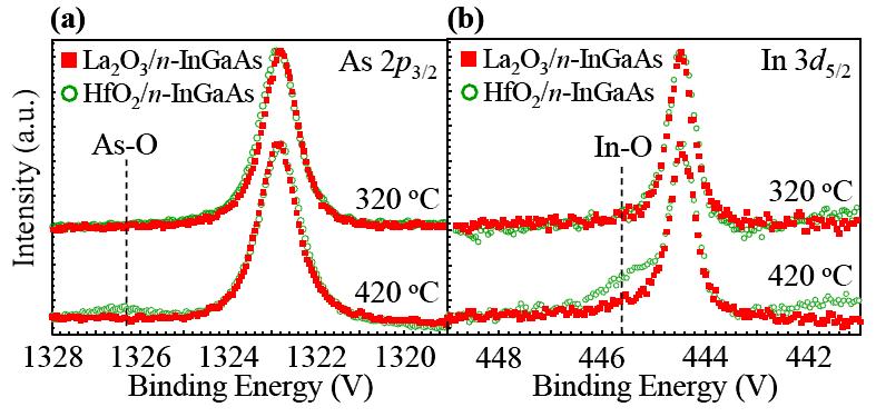
15 XPS 5
16 (p- type) HfO /p- In.53 Ga.47 As MOS CAP K K K (a) -.8 V (b) -. V (c) -.6 V -.4 V - V -.8 V - V -.8 V -.6 V G p /ω (F/cm ) 4.8 V.5 V. V V.8 V V Frequency (Hz) Frequency (Hz) Frequency (Hz) p- type 6
17 k-value La O 3 K eff 5 HfO K eff 9 7
 defect A : oxide bulk traps defect B : interface states 3 4 5 6 defect B defect C V g > E f PMA in F.G.")
18 G p / (µf/cm ) 5.E 6 4.E 6 4.E 6 3.E 6 3.E 6.E 6.E 6.E 6 5.E 7 defect A defect C. V -.7 V defect B.E+ Frequency ( Hz ) defect A : oxide bulk traps defect B : interface states defect B defect C V g > E f PMA in F.G. nm C ox : Interface states : Bulk Trap C acc C it G it C BT G BT W HfO n-in.53 Ga.47 As defects E c E BT E f E i E v W HfO InGaAs defect C : substrate bulk traps 8
19 -3 E BT Time Constant (s) K p-type 3K 4 K n-type 77 K E-E v (ev) V g > E f E f V g < n- type : Bulk Trap : Mid-gap interface traps 3K low temp E c E f E v E c E f E i E v E BT low temp (ψ s >. ev) N D = 7 p- type 9
20 (p- type) HfO /p- In.53 Ga.47 As MOS CAP K K K (a) -.8 V (b) -. V (c) -.6 V -.4 V - V -.8 V - V -.8 V -.6 V G p /ω (F/cm ) 4.8 V.5 V. V V.8 V V Frequency (Hz) Frequency (Hz) Frequency (Hz) p- type
21 τ e = τ t exp( E/ kt) Trapped charge response time Charge carrier trapping time constant: σ τ t = συ t N :capture cross section: 6 cm υ t :thermal velocity: e:5.5 5 h:. 5 Nc ~ = 4.8.( m / m ) T ( cm ) 5 3/ 3/ 3 Γ Nv ~ = 4.8.( m / m ) T ( cm ) 5 3/ 3/ 3 h n N N E k T / i = ( c. v) exp( g /( B )) :. 7 :5.5 8 :~.
22 ~High-k ~ La O 3 /Ge MOS C-V Capacitance (µf/cm ) W La O 3 (5nm) Ge khz khz PMA in N Frequency Dispersion < % peak D it : 5 µm 5 µm cm - ev Gate voltage (V)
23 G p /ω (F/cm ) 5.E E 6 4.E E 6 3.E 6.E 6.E 6.E 6 5.E HfO /InGaAs khz 5 khz Frequency ( Hz ) Gate Voltage ( V ).E+.5 Capacitance (µf/cm ) Hump hysteresis Strech-out Accumulation frequency dispersion Oxide (bulk or border) Interface states Semiconductor bulk C acc C dep C ox C it G it C ox C it G it C BT G BT C ot G ot 3

24 border traps 4
25 D it : G ω p m ox = Gm + ω ( Cox Cm) D it ωgc.5 Gp q ω max 5
26 (D it ) Quasi-static D it D it C-V C-V D it Dieter K. Schroder: Semiconductor Material and Device Characterization 3rd Edition (6). : ~ LSI ~ (99). 6
27 Weak Fermi-level pinning Mid-Gap Dit Mid-Gap 4 o C,5min (with Si) D it [ev - cm - ] o C,5min (with Si) p-type n-type E [ev] 7
28 3nm 3nm () () p-type In.53 Ga.47 As InP n-type In.53 Ga.47 As InP # (p) (n) InGaAs InP (Buffer) Handle 3nm x 7 (Zn) 3nm x 8 (Zn) 5µm 5x 8 (Zn) 3nm 8x 6 (Si) 3nm 3x 8 (Si) 35µm 5x 8 (S) 8
29 .Series Resistance R s (contact, substrate..) measured capacitance C m device capacitance C = ( GR ) ( ) c c s + + ω CR c s parallel conductance (Nicollian&Brews). Fermi Level Pinning) 9
30 τ p = υσ p ps Carrier C it = ( τ ) p Density of holes Hole capture cross secion Hole capture time Accumulation p s capture time( τ p ) C it qd it Depletion τ p C it C = [( C + C ) + C ] tot it sub ox 3
31 InGaAs high-k Al O 3 cm - /ev high-k MG Al O 3 III-V Sub. MG High-k III-V Sub. Al O 3 La O 3 Capacitance ( F/cm ) La O 3 /n-ingaas CV khz khz khz MHz W-FLP D it - - Gate Voltage (V) 3
32 3
 Weak Fermi-level pinning (WFLP) Ref. Martens et. al, MICROELEC.")
33 InGaAs MOS Mid-Gap D it Weak Fermi-level pinning Ref. Hwang et. al, APL. Lett. 96, 9 () Weak Fermi-level pinning (WFLP) Ref. Martens et. al, MICROELEC. 84 (7) Mid-Gap D it Ref. APL. 96, 9 () 33
34 (D it ) Quasi-static D it D it C-V C-V D it Dieter K. Schroder: Semiconductor Material and Device Characterization 3rd Edition (6). : ~ LSI ~ (99). 34
35 La O 3 high-k/si La O 3 ( r =3.4) (E g =5.6eV) Silicate high-k/si 5 o C, 3 min J. A. Ng et al.: IEICE Electronics Express 3 (6) 36 La-silicate La-silicate/Si nm La O 3 35
36 Interface States D it [ev - cm - ] 3 4 o C,5min (with Si) o C,5min (with Si) p-type E [ev] Increasing towards mid-gap More effective for Conduction band Response frequency (Hz).E+ 9.E+9 6.E+6 3.E+3.E+ -3.E-3.E-6-9.E-9 Electron Hole -6 p-type n-type E v Trap energy (ev) E c n-type E g =.74eV 36
37 XPS 37
untitled
 213 74 AlGaN/GaN Influence of metal material on capacitance for Schottky-gated AlGaN/GaN 1, 2, 1, 2, 2, 2, 2, 2, 2, 2, 1, 1 1 AlGaN/GaN デバイス ① GaNの優れた物性値 ② AlGaN/GaN HEMT構造 ワイドバンドギャップ半導体 (3.4eV) 絶縁破壊電界が大きい
PowerPoint プレゼンテーション
 第 61 回応用物理学会 青山学院大学相模原キャンパス 春季学術講演会 2014 年 3 月 18 日 ( 火曜日 ) La 2 O 3 /InGaAs 界面ラフネスに及ぼす ALD プロセスの影響 Impact of ALD process on La 2 O 3 /InGaAs interface roughness 大嶺洋 1,Dariush Hassan Zadeh 1, 角嶋邦之 2, 片岡好則
Conduction Mechanism at Low Temperature of 2-Dimensional Hole Gas at GaN/AlGaN Heterointerface (低温におけるGaN/AlGaN ヘテロ界面の2 次元正孔ガスの伝導機構)
") 2014/03/19 応用物理学会 2014 年春季学術講演会 コンダクタンス法による AlGaN/GaN ヘテロ 接合界面トラップに関する研究 Investigation on interface traps in AlGaN/GaN heterojunction by conductance method 劉璞誠 1, 竇春萌 2, 角嶋邦之 2, 片岡好則 2, 西山彰 2, 杉井信之 2,
2014/03/19 応用物理学会 2014 年春季学術講演会 コンダクタンス法による AlGaN/GaN ヘテロ 接合界面トラップに関する研究 Investigation on interface traps in AlGaN/GaN heterojunction by conductance method 劉璞誠 1, 竇春萌 2, 角嶋邦之 2, 片岡好則 2, 西山彰 2, 杉井信之 2,
MOSFET HiSIM HiSIM2 1
 MOSFET 2007 11 19 HiSIM HiSIM2 1 p/n Junction Shockley - - on-quasi-static - - - Y- HiSIM2 2 Wilson E f E c E g E v Bandgap: E g Fermi Level: E f HiSIM2 3 a Si 1s 2s 2p 3s 3p HiSIM2 4 Fermi-Dirac Distribution
スライド 1
 High-k & Selete 1 2 * * NEC * # * # # 3 4 10 Si/Diamond, Si/SiC, Si/AlOx, Si Si,,, CN SoC, 2007 2010 2013 2016 2019 Materials Selection CZ Defectengineered SOI: Bonded, SIMOX, SOI Emerging Materials Various
1.06μm帯高出力高寿命InGaAs歪量子井戸レーザ
 [email protected] ZnO RPE-MOCVD UV- ZnO MQW LED/PD & Energy harvesting LED ( ) PV & ZnO... 1970 1980 1990 2000 2010 SAW NTT ZnO LN, LT IC PbInAu/PbBi Nb PIN/FET LD/HBT 0.98-1.06m InGaAs QW-LD
スライド 1
 Matsuura Laboratory SiC SiC 13 2004 10 21 22 H-SiC ( C-SiC HOY Matsuura Laboratory n E C E D ( E F E T Matsuura Laboratory Matsuura Laboratory DLTS Osaka Electro-Communication University Unoped n 3C-SiC
PowerPoint プレゼンテーション
 Drain Voltage (mv) 4 2 0-2 -4 0.0 0.2 0.4 0.6 0.8 1.0 Gate Voltage (V) Vds [V] 0.2 0.1 0.0-0.1-0.2-10 -8-6 -4-2 0 Vgs [V] 10 1000 1000 1000 1000 (LSI) Fe Catalyst Fe Catalyst Carbon nanotube 1~2 nm
 hν 688 358 979 309 308.123 Hz α α α α α α No.37 に示す Ti Sa レーザーで実現 術移転も成功し 図 9 に示すよ うに 2 時間は連続測定が可能な システムを実現した Advanced S o l i d S t a t e L a s e r s 2016, JTu2A.26 1-3. 今後は光周波 数比計測装置としてさらに改良 を加えていくとともに
ELECTRONIC IMAGING IN ASTRONOMY Detectors and Instrumentation 5 Instrumentation and detectors
 ELECTRONIC IMAGING IN ASTRONOMY Detectors and Instrumentation 5 Instrumentation and detectors 4 2017/5/10 Contents 5.4 Interferometers 5.4.1 The Fourier Transform Spectrometer (FTS) 5.4.2 The Fabry-Perot
Unidirectional Measurement Current-Shunt Monitor with Dual Comparators (Rev. B
 www.tij.co.jp INA206 INA207 INA208 INA206-INA208 INA206-INA208 V S 1 14 V IN+ V S 1 10 V IN+ OUT CMP1 IN /0.6V REF 2 3 1.2V REF 13 12 V IN 1.2V REF OUT OUT CMP1 IN+ 2 3 9 8 V IN CMP1 OUT CMP1 IN+ 4 11
Triple 2:1 High-Speed Video Multiplexer (Rev. C
 www.tij.co.jp OPA3875 µ ± +5V µ RGB Channel OPA3875 OPA3875 (Patented) RGB Out SELECT ENABLE RED OUT GREEN OUT BLUE OUT 1 R G B RGB Channel 1 R1 G1 B1 X 1 Off Off Off 5V Channel Select EN OPA875 OPA4872
PowerPoint Presentation
 / 2008/04/04 Ferran Salleras 1 2 40Gb/s 40Gb/s PC QD PC: QD: e.g. PCQD PC/QD 3 CP-ON SP T CP-OFF PC/QD-SMZ T ~ps, 40Gb/s ~100fJ T CP-ON CP-OFF 500µm500µm Photonic Crystal SMZ K. Tajima, JJAP, 1993. Control
 2 1 7 - TALK ABOUT 21 μ TALK ABOUT 21 Ag As Se 2. 2. 2. Ag As Se 1 2 3 4 5 6 7 8 9 1 1 2 3 4 5 6 7 8 9 1 1 2 3 4 5 6 7 8 9 1 Sb Ga Te 2. Sb 2. Ga 2. Te 1 2 3 4 5 6 7 8 9 1 1 2 3 4 5 6 7 8 9 1 1 2 3 4
スライド 1
 Front End Processes FEP WG - - NEC 1 ITRS2006 update 2 ITRS vs. 2-1 FET 2-2 Source Drain Extension 2-3 Si-Silicide 2-4 2-5 1 , FEP Front End Processes Starting Materials: FEP Si,, SOI SOI: Si on Insulator,
2
 Rb Rb Rb :10256010 2 3 1 5 1.1....................................... 5 1.2............................................. 5 1.3........................................ 6 2 7 2.1.........................................
Mott散乱によるParity対称性の破れを検証
 Mott Parity P2 Mott target Mott Parity Parity Γ = 1 0 0 0 0 1 0 0 0 0 1 0 0 0 0 1 t P P ),,, ( 3 2 1 0 1 γ γ γ γ γ γ ν ν µ µ = = Γ 1 : : : Γ P P P P x x P ν ν µ µ vector axial vector ν ν µ µ γ γ Γ ν γ
Frontier Simulation Software for Industrial Science
 PACS-CS FIRST 2005 2005 2 16 17 2 28 2 17 2 28 3 IT IT H14~H16 CHASE CHASE-3PT Protein Protein-DF ABINIT-MP 17 2 28 4 CMOS Si-CMOS CMOS-LSI CMOS ATP 10nm 17 2 28 5 17 2 28 6 CMOS CMOS-LSI LSI 90nm CMOS
LT 低コスト、シャットダウン機能付き デュアルおよびトリプル300MHz 電流帰還アンプ
 µ µ LT1398/LT1399 V IN A R G 00Ω CHANNEL A SELECT EN A R F 3Ω B C 97.6Ω CABLE V IN B R G 00Ω EN B R F 3Ω 97.6Ω V OUT OUTPUT (00mV/DIV) EN C V IN C 97.6Ω R G 00Ω R F 3Ω 1399 TA01 R F = R G = 30Ω f = 30MHz
V(x) m e V 0 cos x π x π V(x) = x < π, x > π V 0 (i) x = 0 (V(x) V 0 (1 x 2 /2)) n n d 2 f dξ 2ξ d f 2 dξ + 2n f = 0 H n (ξ) (ii) H
 m e V 0 cos x π x π V(x) = x < π, x > π V 0 (i) x = 0 (V(x) V 0 (1 x 2 /2)) n n d 2 f dξ 2ξ d f 2 dξ + 2n f = 0 H n (ξ) (ii) H") 199 1 1 199 1 1. Vx) m e V cos x π x π Vx) = x < π, x > π V i) x = Vx) V 1 x /)) n n d f dξ ξ d f dξ + n f = H n ξ) ii) H n ξ) = 1) n expξ ) dn dξ n exp ξ )) H n ξ)h m ξ) exp ξ )dξ = π n n!δ n,m x = Vx)
199 1 1 199 1 1. Vx) m e V cos x π x π Vx) = x < π, x > π V i) x = Vx) V 1 x /)) n n d f dξ ξ d f dξ + n f = H n ξ) ii) H n ξ) = 1) n expξ ) dn dξ n exp ξ )) H n ξ)h m ξ) exp ξ )dξ = π n n!δ n,m x = Vx)
µµ InGaAs/GaAs PIN InGaAs PbS/PbSe InSb InAs/InSb MCT (HgCdTe)
") 1001 µµ 1.... 2 2.... 7 3.... 9 4. InGaAs/GaAs PIN... 10 5. InGaAs... 17 6. PbS/PbSe... 18 7. InSb... 22 8. InAs/InSb... 23 9. MCT (HgCdTe)... 25 10.... 28 11.... 29 12. (Si)... 30 13.... 33 14.... 37
1001 µµ 1.... 2 2.... 7 3.... 9 4. InGaAs/GaAs PIN... 10 5. InGaAs... 17 6. PbS/PbSe... 18 7. InSb... 22 8. InAs/InSb... 23 9. MCT (HgCdTe)... 25 10.... 28 11.... 29 12. (Si)... 30 13.... 33 14.... 37
????????????MUX ????????????????????
 PGA116 PGA112 PGA113 PGA117 PGA112, PGA113 PGA116, PGA117 www.tij.co.jp µµ µµ ± µ +5V +3V AV DD 1 C BYPASS.1µF DV DD C BYPASS.1µF C BYPASS.1µF V CAL/CH CH1 3 2 1kΩ MUX CAL1 PGA112 PGA113 R F 1 Output Stage
音響部品アクセサリ本文(AC06)PDF (Page 16)
PDF (Page 16)") Guide for Electret Condenser Microphones A microphone as an audio-electric converting device, whose audio pickup section has a structure of a condenser consisting of a diaphragm and a back plate opposite
Guide for Electret Condenser Microphones A microphone as an audio-electric converting device, whose audio pickup section has a structure of a condenser consisting of a diaphragm and a back plate opposite
 2014.3.10 @stu.hirosaki-u.ac.jp 1 1 1.1 2 3 ( 1) x ( ) 0 1 ( 2)NOT 0 NOT 1 1 NOT 0 ( 3)AND 1 AND 1 3 AND 0 ( 4)OR 0 OR 0 3 OR 1 0 1 x NOT x x AND x x OR x + 1 1 0 x x 1 x 0 x 0 x 1 1.2 n ( ) 1 ( ) n x
XFEL/SPring-8
 DEVELOPMENT STATUS OF RF SYSTEM OF INJECTOR SECTION FOR XFEL/SPRING-8 Takao Asaka 1,A), Takahiro Inagaki B), Hiroyasu Ego A), Toshiaki Kobayashi A), Kazuaki Togawa B), Shinsuke Suzuki A), Yuji Otake B),
AD8212: 高電圧の電流シャント・モニタ
 7 V typ 7 0 V MSOP : 40 V+ V SENSE DC/DC BIAS CIRCUIT CURRENT COMPENSATION I OUT COM BIAS ALPHA 094-00 V PNP 0 7 V typ PNP PNP REV. A REVISION 007 Analog Devices, Inc. All rights reserved. 0-9 -- 0 40
Electrical contact characteristics of n-type diamond with Ti, Ni, NiSi2, and Ni3P electrodes
 Electrical contact characteristics of n-type diamond with Ti, Ni, NiSi 2, and Ni 3 P electrodes 杉井 岩井研究室 12M36240 武正敦 1 注目を集めるワイドギャップ半導体 パワーエレクトロニクス ( 半導体の電力変換分野への応用 ) に期待 ワイドギャップ半導体に注目 Properties (relative
研究成果報告書
 様式 C-19 科学研究費補助金研究成果報告書 平成 21 年 6 月 1 日現在 研究種目 : 若手研究 ( スタートアップ ) 研究期間 :27~28 課題番号 :198624 研究課題名 ( 和文 ) InAlAs 酸化膜による III-V-OIMOS 構造の作製および界面準位に関する研究研究課題名 ( 英文 ) III-V-OIMOSstructurebyusingselectivewetoxidationofInAlAs
mbed祭りMar2016_プルアップ.key
 1 2 4 5 Table 16. Static characteristics (LPC1100, LPC1100L series) continued T amb = 40 C to +85 C, unless otherwise specified. Symbol Parameter Conditions Min Typ [1] Max Unit Standard port pins, RESET
OPA277/2277/4277 (2000.1)
") R OPA OPA OPA OPA OPA OPA OPA OPA OPA µ µ ± ± µ OPA ±± ±± ± µ Offset Trim Offset Trim In OPA +In -Pin DIP, SO- Output NC OPA Out A In A +In A A D Out D In D +In D Out A In A +In A A B Out B In B +In B
R OPA OPA OPA OPA OPA OPA OPA OPA OPA µ µ ± ± µ OPA ±± ±± ± µ Offset Trim Offset Trim In OPA +In -Pin DIP, SO- Output NC OPA Out A In A +In A A D Out D In D +In D Out A In A +In A A B Out B In B +In B
電子部品はんだ接合部の熱疲労寿命解析
 43 Evaluation for Thermal Fatigue Life of Solder Joints in Electronic Components Haruhiko Yamada, Kazuyoshi Ogawa 2 63Sn- 37Pb 95Pb-5Sn Si Cu Si 63Sn-37Pb Since automotive electronic components are used
LMV851/LMV852/LMV854 8 MHz Low Power CMOS, EMI Hardened Operational Amplifi(jp)
") LMV851,LMV852,LMV854 LMV851/LMV852/LMV854 8 MHz Low Power CMOS, EMI Hardened Operational Amplifiers Literature Number: JAJSAM3 LMV851/LMV852/LMV854 8MHz CMOS EMI LMV851/LMV852/LMV854 CMOS IC 40 125 LMV851/
LMV851,LMV852,LMV854 LMV851/LMV852/LMV854 8 MHz Low Power CMOS, EMI Hardened Operational Amplifiers Literature Number: JAJSAM3 LMV851/LMV852/LMV854 8MHz CMOS EMI LMV851/LMV852/LMV854 CMOS IC 40 125 LMV851/
LMC6082 Precision CMOS Dual Operational Amplifier (jp)
") Precision CMOS Dual Operational Amplifier Literature Number: JAJS760 CMOS & CMOS LMC6062 CMOS 19911126 33020 23900 11800 ds011297 Converted to nat2000 DTD Edited for 2001 Databook SGMLFIX:PR1.doc Fixed
Precision CMOS Dual Operational Amplifier Literature Number: JAJS760 CMOS & CMOS LMC6062 CMOS 19911126 33020 23900 11800 ds011297 Converted to nat2000 DTD Edited for 2001 Databook SGMLFIX:PR1.doc Fixed
1 7 ω ω ω 7.1 0, ( ) Q, 7.2 ( Q ) 7.1 ω Z = R +jx Z 1/ Z 7.2 ω 7.2 Abs. admittance (x10-3 S) RLC Series Circuit Y R = 20 Ω L = 100
 Q, 7.2 ( Q ) 7.1 ω Z = R +jx Z 1/ Z 7.2 ω 7.2 Abs. admittance (x10-3 S) RLC Series Circuit Y R = 20 Ω L = 100") 7 7., ) Q, 7. Q ) 7. Z = R +jx Z / Z 7. 7. Abs. admittance x -3 S) 5 4 3 R Series ircuit Y R = Ω = mh = uf Q = 5 5 5 V) Z = R + jx 7. Z 7. ) R = Ω = mh = µf ) 7 V) R Z s = R + j ) 7.3 R =. 7.4) ) f = π.
7 7., ) Q, 7. Q ) 7. Z = R +jx Z / Z 7. 7. Abs. admittance x -3 S) 5 4 3 R Series ircuit Y R = Ω = mh = uf Q = 5 5 5 V) Z = R + jx 7. Z 7. ) R = Ω = mh = µf ) 7 V) R Z s = R + j ) 7.3 R =. 7.4) ) f = π.
?????????????????NMOS?250mA????????????????
 TPS732xx µ µ µ µ µ DBV PACKAGE SOT23 (TOP VIEW) DCQ PACKAGE SOT223 (TOP VIEW) TAB IS GND 1 5 GND 2 1 2 3 4 5 EN 3 4 NR/FB Optional Optional GND EN NR/FB V TPS732xx DRB PACKAGE 3mm x 3mm SON (TOP VIEW)
pc725v0nszxf_j
 PC725NSZXF PC725NSZXF PC725NSZXF PC725 DE file PC725 Date Jun. 3. 25 SHARP Corporation PC725NSZXF 2 6 5 2 3 4 Anode Cathode NC Emitter 3 4 5 Collector 6 Base PC725NSZXF PC725YSZXF.6 ±.2.2 ±.3 SHARP "S"
2004/4/16 (Power Technology) O 2 ( ) (Information Technology) ( ) Gas (4H) GaN andgap (ev) Electron mobility (cm 2 /Vs)
 O 2 ( ) (Information Technology) ( ) Gas (4H) GaN andgap (ev) Electron mobility (cm 2 /Vs)") ontents semicon.kuee.kyoto-u.ac.jp P 5.47 ev 1.12 ev Ge 0.66 ev Sn 0.08 ev DVD LSI, 3.20 ev GaN 3.42 ev ZnO 2004/4/16 (Power Technology) O 2 ( ) (Information Technology) ( ) Gas (4H) GaN andgap (ev) 1.12
ontents semicon.kuee.kyoto-u.ac.jp P 5.47 ev 1.12 ev Ge 0.66 ev Sn 0.08 ev DVD LSI, 3.20 ev GaN 3.42 ev ZnO 2004/4/16 (Power Technology) O 2 ( ) (Information Technology) ( ) Gas (4H) GaN andgap (ev) 1.12
16-Bit, Serial Input Multiplying Digital-to-Analog Converter (Rev. B
 DAC8811 www.tij.co.jp ± ± µ ± µ ± V REF CS Power-On Reset DAC8811 D/A Converter 16 DAC Register 16 R FB I OUT CLK SDI Shift Register GND DAC8811C ±1 ±1 MSOP-8 (DGK) 4to 85 D11 DAC8811ICDGKT DAC8811C ±1
Keysight Technologies B1500Aを使用した太陽電池セルのIV/CV特性評価
 Keysight Technologies B1500A IV/CV Application Note Keysight B1500A IV CV B1500A B1500A 1 pn R sh R s R s R s R sh R sh R s + R sh Cu In Ga Se CIGS 2 DSC C p r p r s + C p r p r s C p C t C d C t C d C
JIS Z803: (substitution method) 3 LCR LCR GPIB
 3 LCR LCR GPIB") LCR NMIJ 003 Agilent 8A 500 ppm JIS Z803:000 50 (substitution method) 3 LCR LCR GPIB Taylor 5 LCR LCR meter (Agilent 8A: Basic accuracy 500 ppm) V D z o I V DUT Z 3 V 3 I A Z V = I V = 0 3 6 V, A LCR meter
LCR NMIJ 003 Agilent 8A 500 ppm JIS Z803:000 50 (substitution method) 3 LCR LCR GPIB Taylor 5 LCR LCR meter (Agilent 8A: Basic accuracy 500 ppm) V D z o I V DUT Z 3 V 3 I A Z V = I V = 0 3 6 V, A LCR meter
Fig. 1. Relation between magnetron anode current and anode-cathod voltage. Fig. 2. Inverter circuit for driving a magnetron. 448 T. IEE Japan, Vol. 11
 High Frequency Inverter for Microwave Oven Norikazu Tokunaga, Member, Yasuo Matsuda, Member, Kunio Isiyama, Non-member (Hitachi, Ltd.), Hisao Amano, Member (Hitachi Engineering, Co., Ltd.). Recently resonant

untitled
 MOSFET 17 1 MOSFET.1 MOS.1.1 MOS.1. MOS.1.3 MOS 4.1.4 8.1.5 9. MOSFET..1 1.. 13..3 18..4 18..5 0..6 1.3 MOSFET.3.1.3. Poon & Yau 3.3.3 LDD MOSFET 5 3.1 3.1.1 6 3.1. 6 3. p MOSFET 3..1 8 3.. 31 3..3 36
JAB RL504:201 JAB NOTE 4 2 January 25, A B
 JAB RL504:201 JAB NOTE 4 JAB RL504:201 2201125 1200025 200-0-25-1/- 2 201-01-25 JAB RL504:201 JAB NOTE 4 2 January 25, 201............... 6 5.1... 6 5.2... 6 5. A... 7 5.4 B... 7 5.5... 8 5.6... 9 5.7...
Microsoft PowerPoint - 14.菅谷修正.pptx
 InGaAs/系量子ドット太陽電池の作製 革新デバイスチーム 菅谷武芳 電子 バンド3:伝導帯 E3 E3 E 正孔 バンド:中間バンド 量子ドット超格子 ミニバンド 量子ドットの井戸型 ポテンシャル バンド:価電子帯 量子ドット太陽電池のバンド図 6%を超える理想的な量子ドット太陽 電池実現には E3として1 9eVが必要 量子ドット超格子太陽電池 理論上 変換効率6%以上 集光 を採用 MBE
devicemondai
 c 2019 i 3 (1) q V I T ε 0 k h c n p (2) T 300 K (3) A ii c 2019 i 1 1 2 13 3 30 4 53 5 78 6 89 7 101 8 112 9 116 A 131 B 132 c 2019 1 1 300 K 1.1 1.5 V 1.1 qv = 1.60 10 19 C 1.5 V = 2.4 10 19 J (1.1)
MOSFET 6-2 CMOS 6-2 TTL Transistor Transistor Logic ECL Emitter Coupled Logic I2L Integrated
 1 -- 7 6 2011 11 1 6-1 MOSFET 6-2 CMOS 6-2 TTL Transistor Transistor Logic ECL Emitter Coupled Logic I2L Integrated Injection Logic 6-3 CMOS CMOS NAND NOR CMOS 6-4 6-5 6-1 6-2 CMOS 6-3 6-4 6-5 c 2011 1/(33)
NJW4108 IC ( ) NJW4108 1cell/2cell IC NJW4108V / Bi-CMOS NJW4108V : SSOP20 P-CHG 1 20 Q-CHG NFB 2 19 CS1 CNT 3 18 CS2 GND 4 17 VS NC 5 16 VREF F-CHG 6
 NJW4108 1cell/2cell IC NJW4108V / Bi-CMOS NJW4108V : SSOP20 P-CHG 1 20 Q-CHG NFB 2 19 CS1 CNT 3 18 CS2 GND 4 17 VS NC 5 16 VREF F-CHG 6") IC ( ) 1cell/2cell IC V / Bi-CMOS V : SSOP20 P-CHG 1 20 Q-CHG NFB 2 19 CS1 CNT 3 18 CS2 GND 4 17 VS NC 5 16 VREF F-CHG 6 15 V + 7 14 TDET 8 13 TH C1 9 12 TL C2 10 11 V - 1 - (Ta=25 C) V + +15 V C1 V C1
IC ( ) 1cell/2cell IC V / Bi-CMOS V : SSOP20 P-CHG 1 20 Q-CHG NFB 2 19 CS1 CNT 3 18 CS2 GND 4 17 VS NC 5 16 VREF F-CHG 6 15 V + 7 14 TDET 8 13 TH C1 9 12 TL C2 10 11 V - 1 - (Ta=25 C) V + +15 V C1 V C1
untitled
 NJM88/A ma.µf SOT-89- TO--(NJM88ADL) ESON6-H(NJM88AKH) NJM88U NJM88ADL NJM88AKH (...97mm) 7dB typ. (f=khz, Vo=V ) Vno=µVrms typ..µf (Vo.7V) Io(max.)=mA Vo±.%.8V typ. (Io=mA ) ON/OFF SOT-89-(NJM88U) / TO--(NJM88ADL)
LTC 自己給電絶縁型コンパレータ
 AC 120V TECCOR 4008L4 OR EUIVALENT NEUTRAL 2N2222 HEATER 25Ω 150Ω 1k 1N4004 2.5k 5W 5.6V R1 680k 390Ω 100µF LE 47k C1 0.01µF ZC ZC COMPARISON > R = R O e B (1/T 1/T O ) B = 3807 1µF THERM 30k YSI 44008
LMC6022 Low Power CMOS Dual Operational Amplifier (jp)
") Low Power CMOS Dual Operational Amplifier Literature Number: JAJS754 CMOS CMOS (100k 5k ) 0.5mW CMOS CMOS LMC6024 100k 5k 120dB 2.5 V/ 40fA Low Power CMOS Dual Operational Amplifier 19910530 33020 23900
Low Power CMOS Dual Operational Amplifier Literature Number: JAJS754 CMOS CMOS (100k 5k ) 0.5mW CMOS CMOS LMC6024 100k 5k 120dB 2.5 V/ 40fA Low Power CMOS Dual Operational Amplifier 19910530 33020 23900

PowerPoint Presentation
 2010 KEK (Japan) (Japan) (Japan) Cheoun, Myun -ki Soongsil (Korea) Ryu,, Chung-Yoe Soongsil (Korea) 1. S.Reddy, M.Prakash and J.M. Lattimer, P.R.D58 #013009 (1998) Magnetar : ~ 10 15 G ~ 10 17 19 G (?)
Plastic Package (Note 12) Note 1: ( ) Top View Order Number T or TF See NS Package Number TA11B for Staggered Lead Non-Isolated Package or TF11B for S
 Note 1: ( ) Top View Order Number T or TF See NS Package Number TA11B for Staggered Lead Non-Isolated Package or TF11B for S") Overture 68W ( ) 0.1 (THD N) 20Hz 20kHz 4 68W 8 38W SPiKe (Self Peak Instantaneous Temperature ( Ke)) SOA (Safe Operating Area) SPiKe 2.0 V ( ) 92dB (min) SN 0.03 THD N IMD (SMTPE) 0.004 V CC 28V 4 68W
Overture 68W ( ) 0.1 (THD N) 20Hz 20kHz 4 68W 8 38W SPiKe (Self Peak Instantaneous Temperature ( Ke)) SOA (Safe Operating Area) SPiKe 2.0 V ( ) 92dB (min) SN 0.03 THD N IMD (SMTPE) 0.004 V CC 28V 4 68W
NJW4124 IC ( ) NJW4124 AC-DC 1cell/2cell IC / 1 NJW4124M / Bi-CMOS NJW4124M : DMP20 P-CHG 1 20 Q-CHG NFB 2 19 CS1 TX-SW 3 18 CS2 GND 4 17 VS PC 5 16 V
 NJW4124 AC-DC 1cell/2cell IC / 1 NJW4124M / Bi-CMOS NJW4124M : DMP20 P-CHG 1 20 Q-CHG NFB 2 19 CS1 TX-SW 3 18 CS2 GND 4 17 VS PC 5 16 V") IC ( ) AC-DC 1cell/2cell IC / 1 M / Bi-CMOS M : DMP20 P-CHG 1 20 Q-CHG NFB 2 19 CS1 TX-SW 3 18 CS2 GND 4 17 VS PC 5 16 VREF ADP 6 15 V + 7 14 TDET 8 13 TH C1 9 12 TL C2 10 11 CHG-SW M - 1 - (Ta=25 C) V
IC ( ) AC-DC 1cell/2cell IC / 1 M / Bi-CMOS M : DMP20 P-CHG 1 20 Q-CHG NFB 2 19 CS1 TX-SW 3 18 CS2 GND 4 17 VS PC 5 16 VREF ADP 6 15 V + 7 14 TDET 8 13 TH C1 9 12 TL C2 10 11 CHG-SW M - 1 - (Ta=25 C) V
fj111_109
 15 1 111 Super Low-Loss / Super High-Density Multi-fiber Optical Connector * * * *2 Katsuki Suematsu Masao Shinoda Takashi Shigenaga Jun Yamakawa *2 *3 *3 Masayoshi Tsukamoto Yoshimi Ono Takayuki Ando
C el = 3 2 Nk B (2.14) c el = 3k B C el = 3 2 Nk B
 c el = 3k B C el = 3 2 Nk B") I [email protected] 217 11 14 4 4.1 2 2.4 C el = 3 2 Nk B (2.14) c el = 3k B 2 3 3.15 C el = 3 2 Nk B 3.15 39 2 1925 (Wolfgang Pauli) (Pauli exclusion principle) T E = p2 2m p T N 4 Pauli Sommerfeld
I [email protected] 217 11 14 4 4.1 2 2.4 C el = 3 2 Nk B (2.14) c el = 3k B 2 3 3.15 C el = 3 2 Nk B 3.15 39 2 1925 (Wolfgang Pauli) (Pauli exclusion principle) T E = p2 2m p T N 4 Pauli Sommerfeld
positron 1930 Dirac 1933 Anderson m 22Na(hl=2.6years), 58Co(hl=71days), 64Cu(hl=12hour) 68Ge(hl=288days) MeV : thermalization m psec 100
, 58Co(hl=71days), 64Cu(hl=12hour) 68Ge(hl=288days) MeV : thermalization m psec 100") positron 1930 Dirac 1933 Anderson m 22Na(hl=2.6years), 58Co(hl=71days), 64Cu(hl=12hour) 68Ge(hl=288days) 0.5 1.5MeV : thermalization 10 100 m psec 100psec nsec E total = 2mc 2 + E e + + E e Ee+ Ee-c mc
positron 1930 Dirac 1933 Anderson m 22Na(hl=2.6years), 58Co(hl=71days), 64Cu(hl=12hour) 68Ge(hl=288days) 0.5 1.5MeV : thermalization 10 100 m psec 100psec nsec E total = 2mc 2 + E e + + E e Ee+ Ee-c mc
B1 Ver ( ), SPICE.,,,,. * : student : jikken. [ ] ( TarouOsaka). (, ) 1 SPICE ( SPICE. *1 OrCAD
![B1 Ver ( ), SPICE.,,,,. * : student : jikken. [ ] ( TarouOsaka). (, ) 1 SPICE ( SPICE. *1 OrCAD](/thumbs/101/152175529.jpg "B1 Ver ( ), SPICE.,,,,. * : student : jikken. [ ] ( TarouOsaka). (, ) 1 SPICE ( SPICE. *1 OrCAD") B1 er. 3.05 (2019.03.27), SPICE.,,,,. * 1 1. 1. 1 1.. 2. : student : jikken. [ ] ( TarouOsaka). (, ) 1 SPICE ( SPICE. *1 OrCAD https://www.orcad.com/jp/resources/orcad-downloads.. 1 2. SPICE 1. SPICE Windows
B1 er. 3.05 (2019.03.27), SPICE.,,,,. * 1 1. 1. 1 1.. 2. : student : jikken. [ ] ( TarouOsaka). (, ) 1 SPICE ( SPICE. *1 OrCAD https://www.orcad.com/jp/resources/orcad-downloads.. 1 2. SPICE 1. SPICE Windows
PowerPoint プレゼンテーション
 () 増幅回路の周波数特性 Frequency characteristic of amplifier circuit (2) 増幅回路の周波数特性 Frequency characteristic of amplifier circuit MOS トランジスタの高周波モデル High-frequency model for MOS FET ゲート酸化膜は薄いので G-S, G-D 間に静電容量が生じる
LM5021 AC-DC Current Mode PWM Controller (jp)
") LM5021 LM5021 AC-DC Current Mode PWM Controller Literature Number: JAJSAC6 LM5021 AC-DC PWM LM5021 (PWM) LM5021 (25 A) 1 ( ENERGY STAR CECP ) Hiccup (Hiccup ) 8 LM5021 100ns 1MHz AC-DC PWM 5021 LM Steve
LM5021 LM5021 AC-DC Current Mode PWM Controller Literature Number: JAJSAC6 LM5021 AC-DC PWM LM5021 (PWM) LM5021 (25 A) 1 ( ENERGY STAR CECP ) Hiccup (Hiccup ) 8 LM5021 100ns 1MHz AC-DC PWM 5021 LM Steve
リードタイプ円板型セラミックコンデンサ(安全規格認定品)樹脂モールド面実装タイプセラミックコンデンサ(安全規格認定品)
樹脂モールド面実装タイプセラミックコンデンサ(安全規格認定品)") !! !! D max. e F±1.0 T max. 25.0 min. 3.0 max. ød (in mm) Lead Code Coating Extension e ød A3 Up to the end of crimp 0.6±0.05 D max. T max. e F±0.8 Lead Code J3 3.5± 1.0 0.5 Coating Extension e ød Up
!! !! D max. e F±1.0 T max. 25.0 min. 3.0 max. ød (in mm) Lead Code Coating Extension e ød A3 Up to the end of crimp 0.6±0.05 D max. T max. e F±0.8 Lead Code J3 3.5± 1.0 0.5 Coating Extension e ød Up
Activation and Control of Electron-Transfer Reactions by Noncovalent Bond
 2 + 4e- + 4 + hν 2 2 1 2 20 J. Am. Chem. oc. Angew. Chem. Int. Ed. umber of Papers 15 10 5 0 1998 1999 2000 2001 2002 2003 Year : J. Am. Chem. oc. (Trost, B. M.; tanford University, UA) 3 π 1/2 k ET =
 5 11 3 1....1 2. 5...4 (1)...5...6...7...17...22 (2)...70...71...72...77...82 (3)...85...86...87...92...97 (4)...101...102...103...112...117 (5)...121...122...123...125...128 1. 10 Web Web WG 5 4 5 ²
. ev=,604k m 3 Debye ɛ 0 kt e λ D = n e n e Ze 4 ln Λ ν ei = 5.6π / ɛ 0 m/ e kt e /3 ν ei v e H + +e H ev Saha x x = 3/ πme kt g i g e n
 003...............................3 Debye................. 3.4................ 3 3 3 3. Larmor Cyclotron... 3 3................ 4 3.3.......... 4 3.3............ 4 3.3...... 4 3.3.3............ 5 3.4.........
(1.2) T D = 0 T = D = 30 kn 1.2 (1.4) 2F W = 0 F = W/2 = 300 kn/2 = 150 kn 1.3 (1.9) R = W 1 + W 2 = = 1100 N. (1.9) W 2 b W 1 a = 0
 T D = 0 T = D = 30 kn 1.2 (1.4) 2F W = 0 F = W/2 = 300 kn/2 = 150 kn 1.3 (1.9) R = W 1 + W 2 = = 1100 N. (1.9) W 2 b W 1 a = 0") 1 1 1.1 1.) T D = T = D = kn 1. 1.4) F W = F = W/ = kn/ = 15 kn 1. 1.9) R = W 1 + W = 6 + 5 = 11 N. 1.9) W b W 1 a = a = W /W 1 )b = 5/6) = 5 cm 1.4 AB AC P 1, P x, y x, y y x 1.4.) P sin 6 + P 1 sin 45
1 1 1.1 1.) T D = T = D = kn 1. 1.4) F W = F = W/ = kn/ = 15 kn 1. 1.9) R = W 1 + W = 6 + 5 = 11 N. 1.9) W b W 1 a = a = W /W 1 )b = 5/6) = 5 cm 1.4 AB AC P 1, P x, y x, y y x 1.4.) P sin 6 + P 1 sin 45
MAX4886 DS.J
 19-0807; Rev 0; 4/07 EVALUATION KIT AVAILABLE μ PART TEMP RANGE PIN- PACKAGE PKG CODE ETO+ -40 C to +85 C 42 TQFN-EP* T42359OM-1 * EYE DIAGRAM ( = 3.3V, f = 2.6GHz 600mV P-P PRBS SIGNAL+) * PRBS = PSUEDORANDOM