PowerPoint プレゼンテーション
|
|
|
- さみ さくいし
- 7 years ago
- Views:
Transcription
 4 2 0-2 -4 0.")

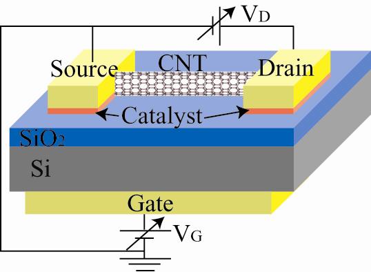
1 Drain Voltage (mv) Gate Voltage (V)
![Vds [V] 0.2 0.1 0.0-0.](/docs-images/97/132902988/images/2-0.jpg "1-0.2-10 -8-6 -4-2 0 Vgs")
2 Vds [V] Vgs [V]
3

")
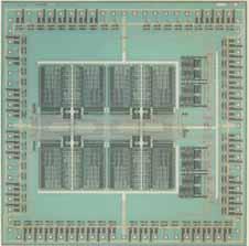
4 (LSI)
5

6

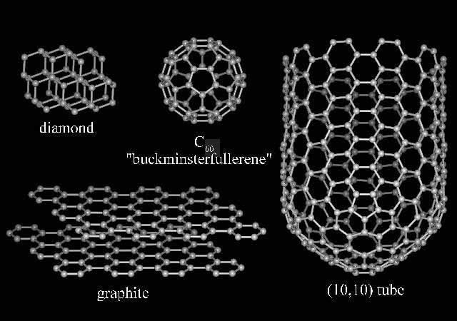
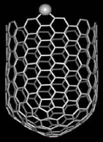
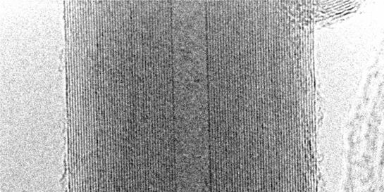
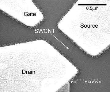
7 Fe Catalyst Fe Catalyst Carbon nanotube 1~2 nm

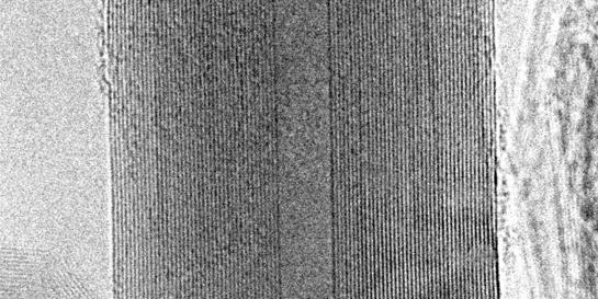
8 ~10nm 0.34nm
9 Scanning Tunneling Microscope (STM) A IBM
10 A E I II III U U = 0 x 1 x 2 x h2 2m d 2 ϕ +U(x) = Eϕ T 2 dx exp 2 h x 2 x 1 2m(E U)dx
11 I II III U ϕ = Aexp ±i h x x 0 2m(E U) dx T = ϕ(iii) ϕ(i) 2 E U = 0 x 1 x 2 x T exp 2 h x 2 x 1 2m(E U)dx L 1 >L 2 T 1 << T 2 STM L 1A T 10 L 1 L 2

12
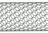
 (2,2) (3,2) (4,2) (5,2) (6,2) armchair zigzag chiral Metal Metal Semi Con. Metal Semi Con. (3,3) (4,3) (5,3) (6,3) (4,4) (5,4)")
13 Chirality of Carbon Nanotube (n, 0) (0,0) (1,0) (2,0) (3,0) (4,0) (5,0) (6,0) (7,0) (1,1) (2,1) (3,1) (4,1) (5,1) (6,1) (7,1) (n,n) (2,2) (3,2) (4,2) (5,2) (6,2) armchair zigzag chiral Metal Metal Semi Con. Metal Semi Con. (3,3) (4,3) (5,3) (6,3) (4,4) (5,4)
14
15
16 Chemical Vapor Deposition (CVD) C Fe C 2 H 5 OH Fe

17 Fe Fe Particle TEM Image of SWCNT Fe CH 4 Gas C C Fe Fe Fe 900C/30min. (Fe)

18 Carbon Nanotube Growth from Fe Particles RT Heating CVD Fe Fe 3 O 4 Fe 2 O 3 Fe 3 O 4 Fe-C CNT FeO Fe 3 C Fe-C
19
 Photo Resist Patterning P.R. Si Sub.")
 Carbon Nanotube Growth Carbon Nanotube CH 4 Gas Si Sub.")
20 Position Controlled Growth of Carbon Nanotube using Patterned Catalyst 1) Photo Resist Patterning P.R. Si Sub. 2) Fe Deposition Fe Si Sub. 3) Lift Off Fe Fe Catalyst Si Sub. 4) Carbon Nanotube Growth Carbon Nanotube CH 4 Gas Si Sub. 900C/30min. Fe Catalyst ~10%

21 Effect of Electric Field on Direction Control of Carbon Nanotube V A CH 4 Gas Catalyst Catalyst Fe Catalyst Fe Catalyst SiO 2 Si Sub. Carbon Nanotube Carbon nanotube Catalyst Catalyst ~20% SiO 2 Si Sub. Effect of Van der Waals Force between Carbon Nanotube & SiO 2 Sub.


22 Effect of Applied Field 0V +20V 0V Growth without Electric field 0V Electric field effect Growth Source 10V Drain -10V Gate -40V


23 + - DC Bias Current Current Time C 2 H 5 OH H 2 CNT 900 Electrode Catalyst Time 900 Current Time


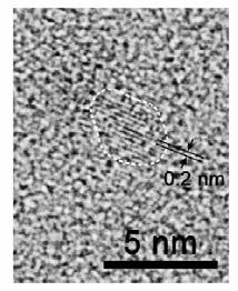

24 1nm
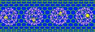
25 Peapod
. K.Hirahara et al., Phys.Rev.Lett. 85, 5384 (2000).")
26 82 peapod Gd +3 EELS Gd Gd K.Hirahara et al., Phys.Rev.Lett. 85, 5384 (2000). K. Suenaga et al., Science 290, 2280 (2000). K.Hirahara et al., Phys.Rev.Lett. 85, 5384 (2000) Ti Ce Gd 92 +6


27 STS - Gd@C 82 Peapod J. Lee et al. Nature (2002) Gd@C 82
28 Peapod FET FET C 60, C 78, C 90 Gd@C 82, Ti 80, etc. Source Peapod Drain Ti/Au SiO 2 (100 nm) + p -Si sub. Hight / nm Length / nm Gate Ti/Au
29 Various Type Peapod FET and its I D -V GS Characteristics I D (A) Ce 2 C 80 -P GdC 82 -P Ti 2 C 80 -P C 60 -P 23 K V DS = 1 mv V GS (V) Ce Ti Gd@C C SWNT FET p Ti 80 FET p / n


30 Various Organic Molecular Doping into Carbon Nanotube CNT CNT Structure was determined by Spring-8.


31
32 MOSFET Metal Oxide Silicon Field Effect Transistor I D : L : Ci : μ ν : Z V G1 Z I Dsat = μ n C i (V G -V T ) 2 2L g m = di Dsat dv G = Z μ n C i (V G -V T ) L V G2 V G3 V G4 L μ n C i Z V D I D I D p L Z p μ p C i p V T V G V T V G


33 Delft University
34 CNT (25,0): 1.99 nm Si GaAs InAs (19,0): 1.51 nm (13,0): 1.03 nm Eg (ev) (cm 2 /Vs) 65,000 35,500 15,000 e: 1,500 h: 450 e: 8,500 h: 400 e: 33,000 h: 460 V. Perebeinos et al. (IBM) PRL 94, (2005) S. M. Sze, Physics of Semiconductor Devices 2nd Ed. Electron Drift Velocity (x10 7 cm/s) Carrier Velocity (10 7 cm/s) 4 CNT 3 2 GaAs Si F (kv/cm) (G. Pennington et al. SISPAD 02, 279 (2002))

 2100 265 g m ( S/ m)")
35 p type Al or Ti Ti SWNT SiO 2 (15nm) g m Si-MOSFET 2 CNT-FET Si-pMOS Lg nm t ox nm V th (V) I on ma/mm) g m ( S/ m)


36 High-k CNT-FET Stanford Univ. A. Javey et al. Nature Mat. 1, 241, ZrO 2 (k ~ 25) : 8 nm SiO 2 (k ~ 3): 0.9 nm p type C G I ON /I OFF ~ 10 4, g m = 6000 μs/μm, s-factor = 70 mv
37 n type Carbon Nanotube FET Logic n FET
38 I D I D p V T V G V T V G


39 FET IBM 52MHz Delft p 5 Hz Stanford 220Hz IBM 52MHz

40 IBM p type n type CNT φ=1.4nm


41 D IBM e h Drain Bias 0 10V(3 sec.) Repeat 190 sec. Integration S
42 D(E) D(E) D(E) E E 1 E 2 E 3 D(E) E E 1 E 2 E 3 D(E) E E 1 E 2 E 3 E
43 1 L x Ly D(E) = 2 dn x dn y dn z de 1 L x L y L z E = h 2 8π 2 m k 2 = h 2 8π 2 m (k 2 x + k 2 y + k 2 z ) L z D(E) = 2 dn x de 1 L x (1) E = h 2 2 k x 8π 2 m = h 2 n x π 8π 2 m L x 2 = n 2 xh 2 2 8mL x L x k x = n xπ L x n x = 2L x 2mE h dn x de = L x h 2m dn x de = L x E h (2) 2m E (1)(2) D(E) = 4 m h 2E 1 2
44 D(E) L x D(E) = 4 m h 2E 1 2 E 1, E 2 E 1 E D(E) D(E) = g s h m 2 E E n ( ) 1 2 E 1 E 2 E 3 E
45 Scanning Tunneling Spectroscopy (STS) J t J t A C B A V V dj t /dv D(E) C B A V
46 Scanning Tunneling Spectroscopy(STS) J t V C B A V Jt Tip E f C B A dj t /dv V J t E f 0 D(E) T(E,V )de D(E) : T(E,V): D(E) C B A V dj t dv D(E) T(E,V ) D(E)


47 STS J t A V
48 (0,0 ) (6,0 ) (5,0 ) (4,0 ) (3,0 ) (2,0 ) (1,0 ) (1,1 ) (7,0 ) (2,1 ) (3,1 ) (4,1 ) (6,1 ) (5,1 ) (7,1 ) (5,2 ) (6,2 ) (4,3 ) (4,4 ) (5,4 ) (5,3 ) (6,3 ) (5,5 ) (2,2 ) (3,2 ) (4,2 ) (3,3 ) Zigzag Type (n,0) Armchair Type (n,n) 1/3 Metalic 2/3 Semiconductor
49 I G 2e 2 h V V
50 E F D(E F ) = g s h m 2 E F E n ( ) 1 2 D(E) E = 1 2 mv 2 v(e F ) = v F = ( ) 2E m = 2 E E F n m 1 2 E 1 E 2 E E F 3 E n I = e D(E F ) v F ev = e g s h m 2 E F E n ( ) E E F n m ( ) 1 2 g ev = s e 2 h V G = I V = g s e2 h = 2e2 h
51 n D(E) I = i= n i=1 2e 2 h V = n 2e2 h V 2e 2 G = I V = 2e2 h h G 3 2 E F E 1 E 2 E 3 E 1 E 1 E 2 E 3 V

52

53 1 R. M. Westervelt Science Nature
54 h2 2m d 2 ϕ +U(x)ϕ = Eϕ 2 dx U= = E 3 ϕ = Csin(kx) = Csin( nπ L x) E 2 k = nπ L = 0 L E 1 x E 3 = 9 8m h 2 L x 2 E n = h2 k 2 2m = h 2 nπ 8π 2 m L 2 = n 2 h 2 8mL 2 E 2 = 4 8m E 1 = 1 8m h 2 L x 2 h 2 L x 2
55 5nm E 3 e GaAs 0 L GaAs E 2 e E 1 GaAlAs GaAlAs x GaAs E 3 e E 2 GaAs A GaAs E 1 GaAs

56 Discrete Energy Level m ΔE Q m m Drain SiO 2 4μm Source

57 Discrete Energy Level K V G =0.98V ΔE Q Drain Source V D =0.4mV SiO 2 4μm Drain Voltage (mv) Drain 4.2 m Source
58 n n+1 ΔE ΔE L E n = hν n = hv F λ n E n +1 λ n +1 E n +1 = hν n +1 = hv F λ n +1 E n λ n ΔE ΔE = E n +1 E n = hv F λ n +1 hv F λ n L = hv F (n +1) 2L hv Fn 2L = hv F 2L
59 Resonant Tunneling of of Hole through Quantum Level in in Carbon Nanotube Negative Conductance Drain Current-Drain Voltage K V G =0.98V V D =0.4mV ΔE Q Discrete Energy Level Drain SiO 2 L 4μm Source ν Drain Voltage (mv) h :Plank s Constant F :Fermi Velocity L :Length of CNT between Tunneling Barriers e :Elementary Charge ΔV D ΔE L = 4.2( μm) ΔE = hν F 2L 1.4μm L : 4.5μm 1 ΔΕ 3
60 35 30 Resonant Tunneling of 1.4μm CNT through Quantum Well 8.6K V G =-3.2V ΔE Q Discrete Energy Level L 25 Drain SiO 2 ΔV Δ 1.4μm D E Q Source 20 V D : V D =1.2mV Drain Voltage (mv) 1.2mV 0.4mV = 3 L =1.4 μm ( ) ΔE ΔV D =1.2mV

 Vg(V) T")

61 W. Liang Harvard Univ. CNT 2LeV c /h ν F = 2 ΔE Q Discrete Energy Level L = 530nm Vg(V) Vg(V) T = 4K L = 200nm Drain SiO 2 4μm Source L = 220nm Vg(V)
62 Single Electron Transistor V G e - e - V D C t C G V G C t V D C Ec = e 2 / 2C E F e - X e/c E F ΔE = (Q-e) 2 /2C - Q 2 /2C = Ec ΔE > 0 Ec > ev e/2c > V Small V D e/2c > V > - e/2c
63 I D E F e - X e/c E F -e/2c e/2c V D Small V D e/2c > V > - e/2c e - I D E F e/c E F -e/2c e/2c V D e/2c < V Large V D V < - e/2c
64 V G e - I D E F e - X e/c E F -e/2c e/2c V D V D I D e/c G Small V D e - I D n = 0 n = 1 E F e/c E F -e/2c V G Gate V G e/2c V D Small V D

65 10K I D -e/2c e/2c V D 0 1 e/2c > V > - e/2c I D e/c G n = 0 n = 1 V G Tunnel Capacitance C 1 = C 2 = 4 x F Gate Capacitance C G = 1 x F
66 1) kt << Ec = e 2 /2C C 2) R T >> h / e 2 = R Q = 26k kt = 26meV at 300K Ec = e 2 /2C = 80meV at C = F r = 10nm 800meV at C = F r = 1nm r E F kt e - X e/c E F -e/2c I D e/2c V D

67 Simulated Charactersitics of Single Electron Tranasistor at 10K & 300K 10K 300K Tunnel Capacitance C 1 = C 2 = 4 x F Gate Capacitance C G = 1 x F C Σ = C 1 + C 2 + C G = 1.8 x F Tunnel Capacitance C 1 = C 2 = 5 x F Gate Capacitance C G = 8 x F
68 4 8.6K Coulomb Diamond Characteristics of of Hole in in Entire Carbon Nanotube Island of of 4.5μm Drain Voltage (mv) n n-1 n-2 n-3 n-4 n-5 n-6 n-7 Drain Current (A) Drain h + Island Source Gate Voltage (V)
![3. Vds [V] SET AFM FIB Voltage pulse 0.2 0.1 0.0-0.1 Drain SiO 2 Si Sub. -0.](/docs-images/97/132902988/images/69-0.jpg "2-10 -8-6 -4-2 0 Vgs [V] + Back Gate AFM CNT Metal coated AFM tip Source ΔV G [V]")
![Ids1[A] 4.0n 3.0n 2.0n 1.0n l =22 nm 0.0-5.0n -10.0n -10-5 0 Vgs[V] 2.6 2.4 2.2 2.0 1.](/docs-images/97/132902988/images/69-1.jpg "8 1.6 1.4 12 14 16 18 20 22 24 Dot length [nm] L = 15 nm CNT 20.0n 15.0n 10.0n 5.0n 0.")
69 3. Vds [V] SET AFM FIB Voltage pulse Drain SiO 2 Si Sub Vgs [V] + Back Gate AFM CNT Metal coated AFM tip Source ΔV G [V] Ids1[A] 4.0n 3.0n 2.0n 1.0n l =22 nm n -10.0n Vgs[V] Dot length [nm] L = 15 nm CNT 20.0n 15.0n 10.0n 5.0n nm/15nm nicks Ids2[A]


70 CNT Single Electron Transistor by AFM Nicking 20K Source e - Gate Drain I D e/c G Island V e 2C 1 n = 0 n = 1 n n -e 2 n 0 n n e 2 Q 0 =C g U g V G -e 2C1


71 CNT Single Electron Transistor by AFM Twisting Source e - Gate Drain 300K Island V e 2C 1 n n -e 2 n 0 n n e 2 Q 0 =C g U g -e 2C1
72


73 (A) ~4V


74 Carbon Nanotube Rope

75 Lightbulbs with Carbon Nanotube Filaments
76 Vds [V] Vgs [V]
MOSFET HiSIM HiSIM2 1
 MOSFET 2007 11 19 HiSIM HiSIM2 1 p/n Junction Shockley - - on-quasi-static - - - Y- HiSIM2 2 Wilson E f E c E g E v Bandgap: E g Fermi Level: E f HiSIM2 3 a Si 1s 2s 2p 3s 3p HiSIM2 4 Fermi-Dirac Distribution
untitled
 213 74 AlGaN/GaN Influence of metal material on capacitance for Schottky-gated AlGaN/GaN 1, 2, 1, 2, 2, 2, 2, 2, 2, 2, 1, 1 1 AlGaN/GaN デバイス ① GaNの優れた物性値 ② AlGaN/GaN HEMT構造 ワイドバンドギャップ半導体 (3.4eV) 絶縁破壊電界が大きい
スライド 1
 Matsuura Laboratory SiC SiC 13 2004 10 21 22 H-SiC ( C-SiC HOY Matsuura Laboratory n E C E D ( E F E T Matsuura Laboratory Matsuura Laboratory DLTS Osaka Electro-Communication University Unoped n 3C-SiC
untitled
 Tokyo Institute of Technology high-k/ In.53 Ga.47 As MOS - Defect Analysis of high-k/in.53 G a.47 As MOS Capacitor using capacitance voltage method,,, Darius Zade,,, Parhat Ahmet,,,,,, ~InGaAs high-k ~
V(x) m e V 0 cos x π x π V(x) = x < π, x > π V 0 (i) x = 0 (V(x) V 0 (1 x 2 /2)) n n d 2 f dξ 2ξ d f 2 dξ + 2n f = 0 H n (ξ) (ii) H
 m e V 0 cos x π x π V(x) = x < π, x > π V 0 (i) x = 0 (V(x) V 0 (1 x 2 /2)) n n d 2 f dξ 2ξ d f 2 dξ + 2n f = 0 H n (ξ) (ii) H") 199 1 1 199 1 1. Vx) m e V cos x π x π Vx) = x < π, x > π V i) x = Vx) V 1 x /)) n n d f dξ ξ d f dξ + n f = H n ξ) ii) H n ξ) = 1) n expξ ) dn dξ n exp ξ )) H n ξ)h m ξ) exp ξ )dξ = π n n!δ n,m x = Vx)
199 1 1 199 1 1. Vx) m e V cos x π x π Vx) = x < π, x > π V i) x = Vx) V 1 x /)) n n d f dξ ξ d f dξ + n f = H n ξ) ii) H n ξ) = 1) n expξ ) dn dξ n exp ξ )) H n ξ)h m ξ) exp ξ )dξ = π n n!δ n,m x = Vx)
Mott散乱によるParity対称性の破れを検証
 Mott Parity P2 Mott target Mott Parity Parity Γ = 1 0 0 0 0 1 0 0 0 0 1 0 0 0 0 1 t P P ),,, ( 3 2 1 0 1 γ γ γ γ γ γ ν ν µ µ = = Γ 1 : : : Γ P P P P x x P ν ν µ µ vector axial vector ν ν µ µ γ γ Γ ν γ
untitled
 MOSFET 17 1 MOSFET.1 MOS.1.1 MOS.1. MOS.1.3 MOS 4.1.4 8.1.5 9. MOSFET..1 1.. 13..3 18..4 18..5 0..6 1.3 MOSFET.3.1.3. Poon & Yau 3.3.3 LDD MOSFET 5 3.1 3.1.1 6 3.1. 6 3. p MOSFET 3..1 8 3.. 31 3..3 36
MOSFET 6-2 CMOS 6-2 TTL Transistor Transistor Logic ECL Emitter Coupled Logic I2L Integrated
 1 -- 7 6 2011 11 1 6-1 MOSFET 6-2 CMOS 6-2 TTL Transistor Transistor Logic ECL Emitter Coupled Logic I2L Integrated Injection Logic 6-3 CMOS CMOS NAND NOR CMOS 6-4 6-5 6-1 6-2 CMOS 6-3 6-4 6-5 c 2011 1/(33)
 1 1 1 1-1 1 1-9 1-3 1-1 13-17 -3 6-4 6 3 3-1 35 3-37 3-3 38 4 4-1 39 4- Fe C TEM 41 4-3 C TEM 44 4-4 Fe TEM 46 4-5 5 4-6 5 5 51 6 5 1 1-1 1991 1,1 multiwall nanotube 1993 singlewall nanotube ( 1,) sp 7.4eV
devicemondai
 c 2019 i 3 (1) q V I T ε 0 k h c n p (2) T 300 K (3) A ii c 2019 i 1 1 2 13 3 30 4 53 5 78 6 89 7 101 8 112 9 116 A 131 B 132 c 2019 1 1 300 K 1.1 1.5 V 1.1 qv = 1.60 10 19 C 1.5 V = 2.4 10 19 J (1.1)
2
 Rb Rb Rb :10256010 2 3 1 5 1.1....................................... 5 1.2............................................. 5 1.3........................................ 6 2 7 2.1.........................................
03_委託テーマ発表資料(その2)(p.89-p.134).pdf
(p.89-p.134).pdf") 89 MEMS 2 / 5-0 0-20 90 3 Beyond-CMOS CNT CNT CNT NEC 4 NEDO (80 NEDO 2008.05 Nature Nanotechnology NEDO (8 22 CNT CNT NEDOPJ CNT NEDO M 3 5 Nature Nanotechnology 3, 289-294 (2008) 6 9 7 8 92 9 (!!! '!!!
89 MEMS 2 / 5-0 0-20 90 3 Beyond-CMOS CNT CNT CNT NEC 4 NEDO (80 NEDO 2008.05 Nature Nanotechnology NEDO (8 22 CNT CNT NEDOPJ CNT NEDO M 3 5 Nature Nanotechnology 3, 289-294 (2008) 6 9 7 8 92 9 (!!! '!!!
W 1983 W ± Z cm 10 cm 50 MeV TAC - ADC ADC [ (µs)] = [] (2.08 ± 0.36) 10 6 s 3 χ µ + µ 8 = (1.20 ± 0.1) 10 5 (Ge
![W 1983 W ± Z cm 10 cm 50 MeV TAC - ADC ADC [ (µs)] = [] (2.08 ± 0.36) 10 6 s 3 χ µ + µ 8 = (1.20 ± 0.1) 10 5 (Ge](/thumbs/91/105929864.jpg "W 1983 W ± Z cm 10 cm 50 MeV TAC - ADC ADC [ (µs)] = [] (2.08 ± 0.36) 10 6 s 3 χ µ + µ 8 = (1.20 ± 0.1) 10 5 (Ge") 22 2 24 W 1983 W ± Z 0 3 10 cm 10 cm 50 MeV TAC - ADC 65000 18 ADC [ (µs)] = 0.0207[] 0.0151 (2.08 ± 0.36) 10 6 s 3 χ 2 2 1 20 µ + µ 8 = (1.20 ± 0.1) 10 5 (GeV) 2 G µ ( hc) 3 1 1 7 1.1.............................
22 2 24 W 1983 W ± Z 0 3 10 cm 10 cm 50 MeV TAC - ADC 65000 18 ADC [ (µs)] = 0.0207[] 0.0151 (2.08 ± 0.36) 10 6 s 3 χ 2 2 1 20 µ + µ 8 = (1.20 ± 0.1) 10 5 (GeV) 2 G µ ( hc) 3 1 1 7 1.1.............................
Muon Muon Muon lif
 2005 2005 3 23 1 2 2 2 2.1 Muon.......................................... 2 2.2 Muon........................... 2 2.3................................. 3 2.4 Muon life time.........................................
ELECTRONIC IMAGING IN ASTRONOMY Detectors and Instrumentation 5 Instrumentation and detectors
 ELECTRONIC IMAGING IN ASTRONOMY Detectors and Instrumentation 5 Instrumentation and detectors 4 2017/5/10 Contents 5.4 Interferometers 5.4.1 The Fourier Transform Spectrometer (FTS) 5.4.2 The Fabry-Perot
positron 1930 Dirac 1933 Anderson m 22Na(hl=2.6years), 58Co(hl=71days), 64Cu(hl=12hour) 68Ge(hl=288days) MeV : thermalization m psec 100
, 58Co(hl=71days), 64Cu(hl=12hour) 68Ge(hl=288days) MeV : thermalization m psec 100") positron 1930 Dirac 1933 Anderson m 22Na(hl=2.6years), 58Co(hl=71days), 64Cu(hl=12hour) 68Ge(hl=288days) 0.5 1.5MeV : thermalization 10 100 m psec 100psec nsec E total = 2mc 2 + E e + + E e Ee+ Ee-c mc
positron 1930 Dirac 1933 Anderson m 22Na(hl=2.6years), 58Co(hl=71days), 64Cu(hl=12hour) 68Ge(hl=288days) 0.5 1.5MeV : thermalization 10 100 m psec 100psec nsec E total = 2mc 2 + E e + + E e Ee+ Ee-c mc
B1 Ver ( ), SPICE.,,,,. * : student : jikken. [ ] ( TarouOsaka). (, ) 1 SPICE ( SPICE. *1 OrCAD
![B1 Ver ( ), SPICE.,,,,. * : student : jikken. [ ] ( TarouOsaka). (, ) 1 SPICE ( SPICE. *1 OrCAD](/thumbs/101/152175529.jpg "B1 Ver ( ), SPICE.,,,,. * : student : jikken. [ ] ( TarouOsaka). (, ) 1 SPICE ( SPICE. *1 OrCAD") B1 er. 3.05 (2019.03.27), SPICE.,,,,. * 1 1. 1. 1 1.. 2. : student : jikken. [ ] ( TarouOsaka). (, ) 1 SPICE ( SPICE. *1 OrCAD https://www.orcad.com/jp/resources/orcad-downloads.. 1 2. SPICE 1. SPICE Windows
B1 er. 3.05 (2019.03.27), SPICE.,,,,. * 1 1. 1. 1 1.. 2. : student : jikken. [ ] ( TarouOsaka). (, ) 1 SPICE ( SPICE. *1 OrCAD https://www.orcad.com/jp/resources/orcad-downloads.. 1 2. SPICE 1. SPICE Windows
13 2 9
 13 9 1 1.1 MOS ASIC 1.1..3.4.5.6.7 3 p 3.1 p 3. 4 MOS 4.1 MOS 4. p MOS 4.3 5 CMOS NAND NOR 5.1 5. CMOS 5.3 CMOS NAND 5.4 CMOS NOR 5.5 .1.1 伝導帯 E C 禁制帯 E g E g E v 価電子帯 図.1 半導体のエネルギー帯. 5 4 伝導帯 E C 伝導電子
 hν 688 358 979 309 308.123 Hz α α α α α α No.37 に示す Ti Sa レーザーで実現 術移転も成功し 図 9 に示すよ うに 2 時間は連続測定が可能な システムを実現した Advanced S o l i d S t a t e L a s e r s 2016, JTu2A.26 1-3. 今後は光周波 数比計測装置としてさらに改良 を加えていくとともに
Frontier Simulation Software for Industrial Science
 PACS-CS FIRST 2005 2005 2 16 17 2 28 2 17 2 28 3 IT IT H14~H16 CHASE CHASE-3PT Protein Protein-DF ABINIT-MP 17 2 28 4 CMOS Si-CMOS CMOS-LSI CMOS ATP 10nm 17 2 28 5 17 2 28 6 CMOS CMOS-LSI LSI 90nm CMOS
QMI_10.dvi
 ... black body radiation black body black body radiation Gustav Kirchhoff 859 895 W. Wien O.R. Lummer cavity radiation ν ν +dν f T (ν) f T (ν)dν = 8πν2 c 3 kt dν (Rayleigh Jeans) (.) f T (ν) spectral energy
スライド 1
 Front End Processes FEP WG - - NEC 1 ITRS2006 update 2 ITRS vs. 2-1 FET 2-2 Source Drain Extension 2-3 Si-Silicide 2-4 2-5 1 , FEP Front End Processes Starting Materials: FEP Si,, SOI SOI: Si on Insulator,
PowerPoint Presentation
 / 2008/04/04 Ferran Salleras 1 2 40Gb/s 40Gb/s PC QD PC: QD: e.g. PCQD PC/QD 3 CP-ON SP T CP-OFF PC/QD-SMZ T ~ps, 40Gb/s ~100fJ T CP-ON CP-OFF 500µm500µm Photonic Crystal SMZ K. Tajima, JJAP, 1993. Control
 http://www.ike-dyn.ritsumei.ac.jp/ hyoo/wave.html 1 1, 5 3 1.1 1..................................... 3 1.2 5.1................................... 4 1.3.......................... 5 1.4 5.2, 5.3....................
Activation and Control of Electron-Transfer Reactions by Noncovalent Bond
 2 + 4e- + 4 + hν 2 2 1 2 20 J. Am. Chem. oc. Angew. Chem. Int. Ed. umber of Papers 15 10 5 0 1998 1999 2000 2001 2002 2003 Year : J. Am. Chem. oc. (Trost, B. M.; tanford University, UA) 3 π 1/2 k ET =
untitled
 SPring-8 RFgun JASRI/SPring-8 6..7 Contents.. 3.. 5. 6. 7. 8. . 3 cavity γ E A = er 3 πε γ vb r B = v E c r c A B A ( ) F = e E + v B A A A A B dp e( v B+ E) = = m d dt dt ( γ v) dv e ( ) dt v B E v E
42 3 u = (37) MeV/c 2 (3.4) [1] u amu m p m n [1] m H [2] m p = (4) MeV/c 2 = (13) u m n = (4) MeV/c 2 =
![42 3 u = (37) MeV/c 2 (3.4) [1] u amu m p m n [1] m H [2] m p = (4) MeV/c 2 = (13) u m n = (4) MeV/c 2 =](/thumbs/73/68712188.jpg "42 3 u = (37) MeV/c 2 (3.4) [1] u amu m p m n [1] m H [2] m p = (4) MeV/c 2 = (13) u m n = (4) MeV/c 2 =") 3 3.1 3.1.1 kg m s J = kg m 2 s 2 MeV MeV [1] 1MeV=1 6 ev = 1.62 176 462 (63) 1 13 J (3.1) [1] 1MeV/c 2 =1.782 661 731 (7) 1 3 kg (3.2) c =1 MeV (atomic mass unit) 12 C u = 1 12 M(12 C) (3.3) 41 42 3 u
3 3.1 3.1.1 kg m s J = kg m 2 s 2 MeV MeV [1] 1MeV=1 6 ev = 1.62 176 462 (63) 1 13 J (3.1) [1] 1MeV/c 2 =1.782 661 731 (7) 1 3 kg (3.2) c =1 MeV (atomic mass unit) 12 C u = 1 12 M(12 C) (3.3) 41 42 3 u
4_Laser.dvi
 1 1905 A.Einstein 1917 A.Einstein 1954 C.H.Townes MASER Microwave Amplification by Stimulated Emission of Radiation 23.9 GHz 1.26 cm 1960 T.H.Maiman LASER Light Amplification by Stimulated Emissin of Radiation
 B 1 B.1.......................... 1 B.1.1................. 1 B.1.2................. 2 B.2........................... 5 B.2.1.......................... 5 B.2.2.................. 6 B.2.3..................
. ev=,604k m 3 Debye ɛ 0 kt e λ D = n e n e Ze 4 ln Λ ν ei = 5.6π / ɛ 0 m/ e kt e /3 ν ei v e H + +e H ev Saha x x = 3/ πme kt g i g e n
 003...............................3 Debye................. 3.4................ 3 3 3 3. Larmor Cyclotron... 3 3................ 4 3.3.......... 4 3.3............ 4 3.3...... 4 3.3.3............ 5 3.4.........
(4.15a) Hurwitz (4.15a) {a j } (s ) {a j } n n Hurwitz a n 1 a n 3 a n 5 a n a n 2 a n 4 a n 1 a n 3 H = a n a n 2. (4.16)..... a Hurwitz H i H i i H
 Hurwitz (4.15a) {a j } (s ) {a j } n n Hurwitz a n 1 a n 3 a n 5 a n a n 2 a n 4 a n 1 a n 3 H = a n a n 2. (4.16)..... a Hurwitz H i H i i H") 6 ( ) 218 1 28 4.2.6 4.1 u(t) w(t) K w(t) = Ku(t τ) (4.1) τ Ξ(iω) = exp[ α(ω) iβ(ω)] (4.11) (4.1) exp[ α(ω) iβ(ω)] = K exp( iωτ) (4.12) α(ω) = ln(k), β(ω) = ωτ (4.13) dϕ/dω f T 4.3 ( ) OP-amp Nyquist Hurwitz
6 ( ) 218 1 28 4.2.6 4.1 u(t) w(t) K w(t) = Ku(t τ) (4.1) τ Ξ(iω) = exp[ α(ω) iβ(ω)] (4.11) (4.1) exp[ α(ω) iβ(ω)] = K exp( iωτ) (4.12) α(ω) = ln(k), β(ω) = ωτ (4.13) dϕ/dω f T 4.3 ( ) OP-amp Nyquist Hurwitz
untitled
 (a) (b) (c) (d) Wunderlich 2.5.1 = = =90 2 1 (hkl) {hkl} [hkl] L tan 2θ = r L nλ = 2dsinθ dhkl ( ) = 1 2 2 2 h k l + + a b c c l=2 l=1 l=0 Polanyi nλ = I sinφ I: B A a 110 B c 110 b b 110 µ a 110
 http://www.ns.kogakuin.ac.jp/~ft13389/lecture/physics1a2b/ pdf I 1 1 1.1 ( ) 1. 30 m µm 2. 20 cm km 3. 10 m 2 cm 2 4. 5 cm 3 km 3 5. 1 6. 1 7. 1 1.2 ( ) 1. 1 m + 10 cm 2. 1 hr + 6400 sec 3. 3.0 10 5 kg
note4.dvi
 10 016 6 0 4 (quantum wire) 4.1 4.1.1.6.1, 4.1(a) V Q N dep ( ) 4.1(b) w σ E z (d) E z (d) = σ [ ( ) ( )] x w/ x+w/ π+arctan arctan πǫǫ 0 d d (4.1) à ƒq [ƒg w ó R w d V( x) QŽŸŒ³ džq x (a) (b) 4.1 (a)
原子・分子架橋系の量子輸送の理論 現状と展望
 1cm 10 21 1 m 1nm 10 9 1 10-4 N Maxwell DFT E.Tsuchida and M.Tsukada Phys.Rev.B52(1995)5573-5578 Phys.Rev.B54(1996)7602-7605 J.Phys.Soc.Jpn.67(1998)3844-3858 Chem.Phys.Lett.311(1999)236-240 N.Watanabe
25 3 4
 25 3 4 1 µ e + ν e +ν µ µ + e + +ν e + ν µ e e + TAC START STOP START veto START (2.04 ± 0.18)µs 1/2 STOP (2.09 ± 0.11)µs 1/8 G F /( c) 3 (1.21±0.09) 5 /GeV 2 (1.19±0.05) 5 /GeV 2 Weinberg θ W sin θ W
 = hυ = h c λ υ λ (ev) = 1240 λ W=NE = Nhc λ W= N 2 10-16 λ / / Φe = dqe dt J/s Φ = km Φe(λ)v(λ)dλ THBV3_0101JA Qe = Φedt (W s) Q = Φdt lm s Ee = dφe ds E = dφ ds Φ Φ THBV3_0102JA Me = dφe ds M = dφ ds
電子回路I_4.ppt
 電子回路 Ⅰ 第 4 回 電子回路 Ⅰ 5 1 講義内容 1. 半導体素子 ( ダイオードとトランジスタ ) 2. 基本回路 3. 増幅回路 電界効果トランジスタ (FET) 基本構造 基本動作動作原理 静特性 電子回路 Ⅰ 5 2 半導体素子 ( ダイオードとトランジスタ ) ダイオード (2 端子素子 ) トランジスタ (3 端子素子 ) バイポーラトランジスタ (Biolar) 電界効果トランジスタ
i
 009 I 1 8 5 i 0 1 0.1..................................... 1 0.................................................. 1 0.3................................. 0.4........................................... 3
スライド 1
 High-k & Selete 1 2 * * NEC * # * # # 3 4 10 Si/Diamond, Si/SiC, Si/AlOx, Si Si,,, CN SoC, 2007 2010 2013 2016 2019 Materials Selection CZ Defectengineered SOI: Bonded, SIMOX, SOI Emerging Materials Various
p = mv p x > h/4π λ = h p m v Ψ 2 Ψ
 II p = mv p x > h/4π λ = h p m v Ψ 2 Ψ Ψ Ψ 2 0 x P'(x) m d 2 x = mω 2 x = kx = F(x) dt 2 x = cos(ωt + φ) mω 2 = k ω = m k v = dx = -ωsin(ωt + φ) dt = d 2 x dt 2 0 y v θ P(x,y) θ = ωt + φ ν = ω [Hz] 2π
<4D F736F F D B B83578B6594BB2D834A836F815B82D082C88C602E646F63>
 スピントロニクスの基礎 サンプルページ この本の定価 判型などは, 以下の URL からご覧いただけます. http://www.morikita.co.jp/books/mid/077461 このサンプルページの内容は, 初版 1 刷発行時のものです. i 1 2 ii 3 5 4 AMR (anisotropic magnetoresistance effect) GMR (giant magnetoresistance
Bethe-Bloch Bethe-Bloch (stopping range) Bethe-Bloch FNAL (Fermi National Accelerator Laboratory) - (SciBooNE ) SciBooNE Bethe-Bloch FNAL - (SciBooNE
 Bethe-Bloch FNAL (Fermi National Accelerator Laboratory) - (SciBooNE ) SciBooNE Bethe-Bloch FNAL - (SciBooNE") 21 2 27 Bethe-Bloch Bethe-Bloch (stopping range) Bethe-Bloch FNAL (Fermi National Accelerator Laboratory) - (SciBooNE ) SciBooNE Bethe-Bloch FNAL - (SciBooNE ) Bethe-Bloch 1 0.1..............................
21 2 27 Bethe-Bloch Bethe-Bloch (stopping range) Bethe-Bloch FNAL (Fermi National Accelerator Laboratory) - (SciBooNE ) SciBooNE Bethe-Bloch FNAL - (SciBooNE ) Bethe-Bloch 1 0.1..............................
untitled
 2008-11/13 12 4 12 5 401 501 702 401 501 A-1 9:00-10:30 B-1 9:15-10:30 C-1 9:00-10:30 A-5 9:00-10:30 B-5 9:15-10:30 A A-2 10:45-12:15 B-2 10:45-12:15 C-2 10:45-12:15 A-6 10:45-12:15 B-6 10:45-12:15 A B
10 nm SThM Fig.1 AFM 6) AFM 7) Fig.1 AFM 0.1 N/m 100 pn 10 nn 8) SThM STM AFM RTD Resistance Temperature Device SNOM Scanning Near-field Optical Micro
 AFM 7) Fig.1 AFM 0.1 N/m 100 pn 10 nn 8) SThM STM AFM RTD Resistance Temperature Device SNOM Scanning Near-field Optical Micro") @@@@@@@@@@@@@@ @@@@@@@@@@@@@@@@@@@@@@@@@@@@@@@@@@@@@@@@@@@@@@@@@@@@@@@@@@@@@@@@@@@@@@@@@@@@@@@@@@@@@@@@@@@@@@@@@@@@@@@@@@@@@@@@@@@@@@@@@@@@@@@@@@@@@@@@@@@@@@@@@@@@@@@@@@@@@@@@@@@@@@@@@@@@@@@@@@@@@@@@@@@@@@@@@@@@@@@@@@@@@@@@
@@@@@@@@@@@@@@ @@@@@@@@@@@@@@@@@@@@@@@@@@@@@@@@@@@@@@@@@@@@@@@@@@@@@@@@@@@@@@@@@@@@@@@@@@@@@@@@@@@@@@@@@@@@@@@@@@@@@@@@@@@@@@@@@@@@@@@@@@@@@@@@@@@@@@@@@@@@@@@@@@@@@@@@@@@@@@@@@@@@@@@@@@@@@@@@@@@@@@@@@@@@@@@@@@@@@@@@@@@@@@@@
1 9 v.0.1 c (2016/10/07) Minoru Suzuki T µ 1 (7.108) f(e ) = 1 e β(e µ) 1 E 1 f(e ) (Bose-Einstein distribution function) *1 (8.1) (9.1)
 Minoru Suzuki T µ 1 (7.108) f(e ) = 1 e β(e µ) 1 E 1 f(e ) (Bose-Einstein distribution function) *1 (8.1) (9.1)") 1 9 v..1 c (216/1/7) Minoru Suzuki 1 1 9.1 9.1.1 T µ 1 (7.18) f(e ) = 1 e β(e µ) 1 E 1 f(e ) (Bose-Einstein distribution function) *1 (8.1) (9.1) E E µ = E f(e ) E µ (9.1) µ (9.2) µ 1 e β(e µ) 1 f(e )
1 9 v..1 c (216/1/7) Minoru Suzuki 1 1 9.1 9.1.1 T µ 1 (7.18) f(e ) = 1 e β(e µ) 1 E 1 f(e ) (Bose-Einstein distribution function) *1 (8.1) (9.1) E E µ = E f(e ) E µ (9.1) µ (9.2) µ 1 e β(e µ) 1 f(e )
From Evans Application Notes
 3 From Evans Application Notes http://www.eaglabs.com From Evans Application Notes http://www.eaglabs.com XPS AES ISS SSIMS ATR-IR 1-10keV µ 1 V() r = kx 2 = 2π µν x mm 1 2 µ= m + m 1 2 1 k ν = OSC 2
news
 ETL NEWS 1999.9 ETL NEWS 1999.11 Establishment of an Evaluation Technique for Laser Pulse Timing Fluctuations Optoelectronics Division Hidemi Tsuchida e-mail:[email protected] A new technique has been
untitled
 (a) (b) (c) (d) (e) (f) (g) (f) (a), (b) 1 He Gleiter 1) 5-25 nm 1/2 Hall-Petch 10 nm Hall-Petch 2) 3) 4) 2 mm 5000% 5) 1(e) 20 µm Pd, Zr 1(f) Fe 6) 10 nm 2 8) Al-- 1,500 MPa 9) 2 Fe 73.5 Si 13.5 B 9 Nb
 Laser Ablation Dynamics of Amorphous Film of a Cu-Phthalocyanine Derivative Masahiro HOSODA*,**, Hiroshi FURUTANI*,**. Hiroshi FUKUMURA*,** Hiroshi MASUHARA*, Masanobu NISHII*** Nobuyuki ICHINOSE**,***,

物理化学I-第12回(13).ppt
.ppt") I- 12-1 11 11.1 2Mg(s) + O 2 (g) 2MgO(s) [Mg 2+ O 2 ] Zn(s) + Cu 2+ (aq) Zn 2+ (aq) + Cu(s) - 2Mg(s) 2Mg 2+ (s) + 4e +) O 2 (g) + 4e 2O 2 (s) 2Mg(s) + O 2 (g) 2MgO(s) Zn(s) Zn 2+ (aq) + 2e +) Cu 2+ (aq)
I- 12-1 11 11.1 2Mg(s) + O 2 (g) 2MgO(s) [Mg 2+ O 2 ] Zn(s) + Cu 2+ (aq) Zn 2+ (aq) + Cu(s) - 2Mg(s) 2Mg 2+ (s) + 4e +) O 2 (g) + 4e 2O 2 (s) 2Mg(s) + O 2 (g) 2MgO(s) Zn(s) Zn 2+ (aq) + 2e +) Cu 2+ (aq)
1-2 原子層制御量子ナノ構造のコヒーレント量子効果 Coherent Quantum Effects in Quantum Nano-structure with Atomic Layer Precision Mutsuo Ogura, Research Director of CREST Pho
 1-2 原子層制御量子ナノ構造のコヒーレント量子効果 Coherent Quantum Effects in Quantum Nano-structure with Atomic Layer Precision Mutsuo Ogura, Research Director of CREST Photonics Research Institute, AIST TBAs) AlGaAs/GaAs TBAs)
PowerPoint プレゼンテーション
 第 61 回応用物理学会 青山学院大学相模原キャンパス 春季学術講演会 2014 年 3 月 18 日 ( 火曜日 ) La 2 O 3 /InGaAs 界面ラフネスに及ぼす ALD プロセスの影響 Impact of ALD process on La 2 O 3 /InGaAs interface roughness 大嶺洋 1,Dariush Hassan Zadeh 1, 角嶋邦之 2, 片岡好則
(1.2) T D = 0 T = D = 30 kn 1.2 (1.4) 2F W = 0 F = W/2 = 300 kn/2 = 150 kn 1.3 (1.9) R = W 1 + W 2 = = 1100 N. (1.9) W 2 b W 1 a = 0
 T D = 0 T = D = 30 kn 1.2 (1.4) 2F W = 0 F = W/2 = 300 kn/2 = 150 kn 1.3 (1.9) R = W 1 + W 2 = = 1100 N. (1.9) W 2 b W 1 a = 0") 1 1 1.1 1.) T D = T = D = kn 1. 1.4) F W = F = W/ = kn/ = 15 kn 1. 1.9) R = W 1 + W = 6 + 5 = 11 N. 1.9) W b W 1 a = a = W /W 1 )b = 5/6) = 5 cm 1.4 AB AC P 1, P x, y x, y y x 1.4.) P sin 6 + P 1 sin 45
1 1 1.1 1.) T D = T = D = kn 1. 1.4) F W = F = W/ = kn/ = 15 kn 1. 1.9) R = W 1 + W = 6 + 5 = 11 N. 1.9) W b W 1 a = a = W /W 1 )b = 5/6) = 5 cm 1.4 AB AC P 1, P x, y x, y y x 1.4.) P sin 6 + P 1 sin 45
1/2 ( ) 1 * 1 2/3 *2 up charm top -1/3 down strange bottom 6 (ν e, ν µ, ν τ ) -1 (e) (µ) (τ) 6 ( 2 ) 6 6 I II III u d ν e e c s ν µ µ t b ν τ τ (2a) (
 1 * 1 2/3 *2 up charm top -1/3 down strange bottom 6 (ν e, ν µ, ν τ ) -1 (e) (µ) (τ) 6 ( 2 ) 6 6 I II III u d ν e e c s ν µ µ t b ν τ τ (2a) (") August 26, 2005 1 1 1.1...................................... 1 1.2......................... 4 1.3....................... 5 1.4.............. 7 1.5.................... 8 1.6 GIM..........................
August 26, 2005 1 1 1.1...................................... 1 1.2......................... 4 1.3....................... 5 1.4.............. 7 1.5.................... 8 1.6 GIM..........................
PowerPoint Presentation
 2010 KEK (Japan) (Japan) (Japan) Cheoun, Myun -ki Soongsil (Korea) Ryu,, Chung-Yoe Soongsil (Korea) 1. S.Reddy, M.Prakash and J.M. Lattimer, P.R.D58 #013009 (1998) Magnetar : ~ 10 15 G ~ 10 17 19 G (?)
untitled
 27.2.9 TOF-SIMS SIMS TOF-SIMS SIMS Mass Spectrometer ABCDE + ABC+ DE + Primary Ions: 1 12 ions/cm 2 Molecular Fragmentation Region ABCDE ABCDE 1 15 atoms/cm 2 Molecular Desorption Region Why TOF-SIMS?