スライド 1
|
|
|
- はすな ことじ
- 7 years ago
- Views:
Transcription

1 1
2 1. 2
3 2. 3


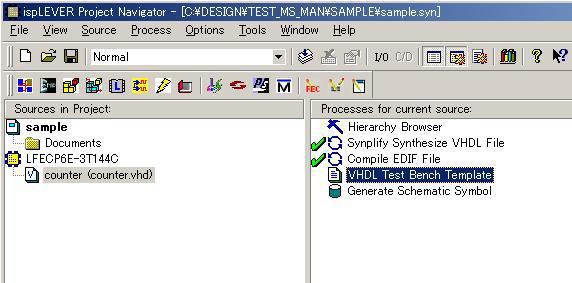
4 isplever 4
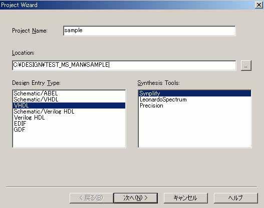
5 5
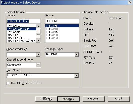
6 6
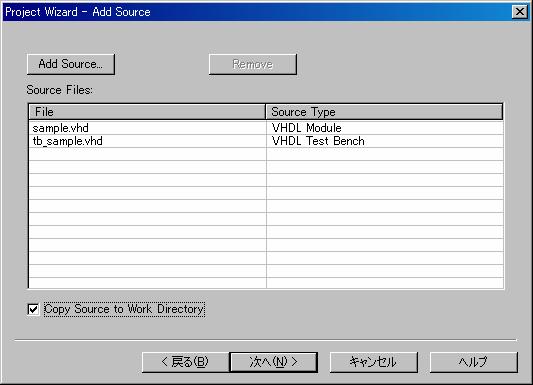
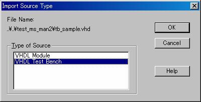
7 7
8 8
9 9
10 VHDL 10
11 VHDL 4 Decode cnt = "1010" High Low DOUT CLK 25MHz 50MHz clk_inst Cnt[3:0] RST
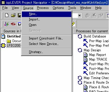
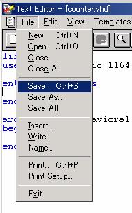
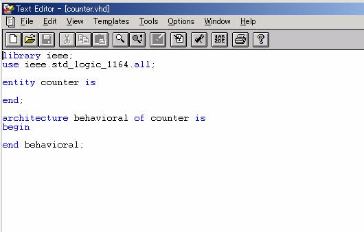
12 library ieee; library xp; use xp.components.all; use ieee.std_logic_1164.all; use ieee.std_logic_arith.all; use ieee.std_logic_unsigned.all; entity top is port( ); end; architecture behavioral of top is RST,CLK : in std_logic; DOUT : out std_logic component pll_inst port (CLK: in std_logic; RESET: in std_logic; CLKOP: out std_logic; LOCK: out std_logic); end component; signal cnt : std_logic_vector(3 downto 0); signal clk_inst : std_logic; signal lock : std_logic; signal pll_rst : std_logic; begin VHDL pll_rst <= not RST; -- parameterized module component instance PLL_UUT : pll_inst port map (CLK => CLK, RESET => pll_rst, CLKOP => clk_inst, LOCK => lock); process(clk_inst,rst) begin if((rst = '0') or (lock = '0'))then cnt <= (others => '0'); elsif(clk_inst'event and clk_inst = '1')then cnt <= cnt + 1; end if; end process; DOUT <= '1' when cnt = "1010" else '0'; end behavioral; 12


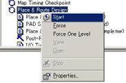
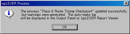
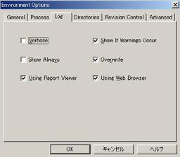
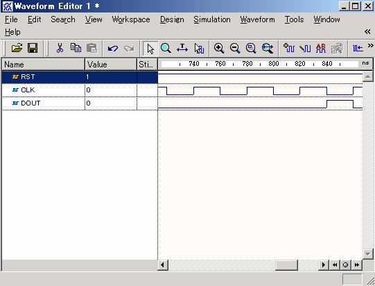
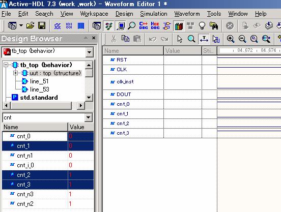
13 ( ) 1. Place & Route Timing Checkpoint Start 2. [Start] ( ) ( ) ( ) 13
14 14
15 15
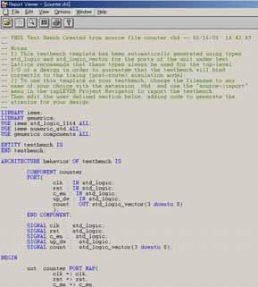
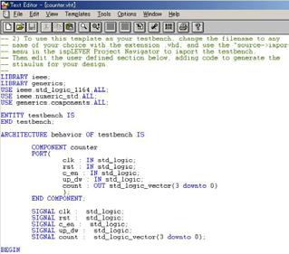
16 LIBRARY ieee; USE ieee.std_logic_1164.all; USE ieee.numeric_std.all; ENTITY tb_top IS END tb_top; ARCHITECTURE behavior OF tb_top IS BEGIN COMPONENT top PORT( RST : IN std_logic; CLK : IN std_logic; DOUT : OUT std_logic ); END COMPONENT; SIGNAL RST : std_logic; SIGNAL CLK : std_logic := '0'; SIGNAL DOUT : std_logic; uut: top PORT MAP( RST => RST, CLK => CLK, DOUT => DOUT ); CLK <= not (CLK) after 20 ns; 25MHz 10ns RST = 0 RST = 1 process begin end process; END; RST <= '0'; wait for 10 ns; RST <= '1'; wait; 16
17 17

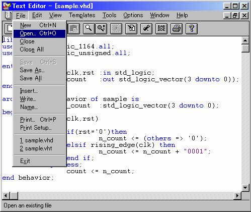
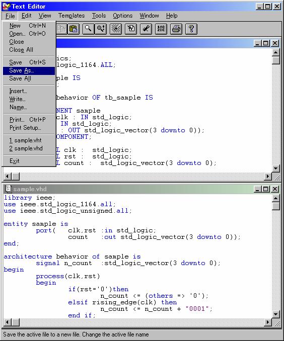
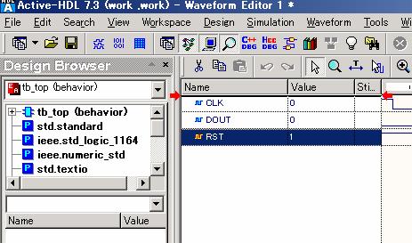
18 1.Project Navigator VHDL Functional Simulation With Aldec Active-HDL or VHDL Post-Route Functional Simulation With Aldec Active-HDL or VHDL Post-Route Timing Simulation With Aldec Active-HDL Active-HDL 2.Active-HDL 18

19 3. Undock wave wave view 19
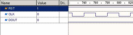
20 RST 20

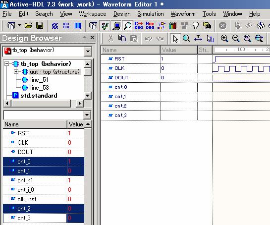
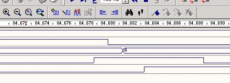
21 uut uut cnt0 cnt3 Cntl 21
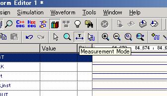
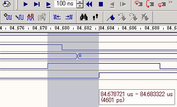
![[ ]](/docs-images/91/105556991/images/22-1.jpg "[Merge")
![Signals]](/docs-images/91/105556991/images/22-2.jpg "+ 22")
22 [ ] [Merge Signals] + 22

23 restart Run restart 23

24 uut cnt cnt 24
")

25 General OK ( Binary ) cnt Properties Binary 25


26 Display OK Display Height Color Bold Shape Literal Logic High Low Analog 26


27 General Edit Aliases Signal Alias Editor Alias_name Value Mnemonic cnt Signal Alias Use Alias Signal Alias Editor 27


28 Waveform editor Zoom Mode 28
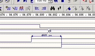
29 Measurement Mode 4.6ns 29
.")

30 Active-HDL GUI Files Console Active-HDL do -tcl ( ).fado VHDL Functional Simulation do -tcl ( ).xado VHDL Post-Route Functional Simulation do -tcl ( ).xado VHDL Post-Route Timing Simulation do -tcl.vado Velirog Functional Simulation do -tcl. ado Velirog Post-Route Functional Simulation do -tcl.wado Velirog Post-Route Timing Simulation 30


31 Active-HDL Stimulators Typer Typer Display Paths Apply CLK Type Clock 10MH 31


32 Signal Breakpoints cnt_3 Simulation Breakpoints 32

33 -break always : -break when less : Hit count -break when equal : Hit count -break when grater : Hit count -break when multiple of: Hit count 33

34 run cnt3 = 1 Break run cnt3 = 1 Break 34


35 Active-HDL Active-HDL View Library_Manager Attach Library *.lib Attach as Global Library 35


36 VCD VCD Export File Export Waveforms VCD for Verilogdesign : Verilog VCD VCD for VHDL design : VDHL VCD VCD Lattice Power Calucrator VCD 36


37 JPG BMP GIF PNG File Export Grafics OK 37
38 FAE /FAX URL 38
39 Revision History 39
スライド 1
 isplever CLASIC 1.2 Startup Manual for MACH4000 Rev.1.0 isplever_ CLASIC Startup_for_MACH4000_Rev01.ppt Page: 1 1. Page 3 2. Lattice isplever Design Flow Page 4 3. Page 5 3-1 Page 6 3-2 Page 7 3-3 Page
if clear = 1 then Q <= " "; elsif we = 1 then Q <= D; end rtl; regs.vhdl clk 0 1 rst clear we Write Enable we 1 we 0 if clk 1 Q if rst =
 VHDL 2 1 VHDL 1 VHDL FPGA VHDL 2 HDL VHDL 2.1 D 1 library ieee; use ieee.std_logic_1164.all; use ieee.std_logic_unsigned.all; regs.vhdl entity regs is clk, rst : in std_logic; clear : in std_logic; we
1 1 2 2 2-1 2 2-2 4 2-3 11 2-4 12 2-5 14 3 16 3-1 16 3-2 18 3-3 22 4 35 4-1 VHDL 35 4-2 VHDL 37 4-3 VHDL 37 4-3-1 37 4-3-2 42 i
 1030195 15 2 10 1 1 2 2 2-1 2 2-2 4 2-3 11 2-4 12 2-5 14 3 16 3-1 16 3-2 18 3-3 22 4 35 4-1 VHDL 35 4-2 VHDL 37 4-3 VHDL 37 4-3-1 37 4-3-2 42 i 4-3-3 47 5 52 53 54 55 ii 1 VHDL IC VHDL 5 2 3 IC 4 5 1 2
Unconventional HDL Programming ( version) 1
 1") Unconventional HDL Programming (20090425 version) 1 1 Introduction HDL HDL Hadware Description Language printf printf (C ) HDL 1 HDL HDL HDL HDL HDL HDL 1 2 2 2.1 VHDL 1 library ieee; 2 use ieee.std_logic_1164.all;
Unconventional HDL Programming (20090425 version) 1 1 Introduction HDL HDL Hadware Description Language printf printf (C ) HDL 1 HDL HDL HDL HDL HDL HDL 1 2 2 2.1 VHDL 1 library ieee; 2 use ieee.std_logic_1164.all;
VHDL
 VHDL 1030192 15 2 10 1 1 2 2 2.1 2 2.2 5 2.3 11 2.3.1 12 2.3.2 12 2.4 12 2.4.1 12 2.4.2 13 2.5 13 2.5.1 13 2.5.2 14 2.6 15 2.6.1 15 2.6.2 16 3 IC 17 3.1 IC 17 3.2 T T L 17 3.3 C M O S 20 3.4 21 i 3.5 21
TECH_I Vol.25 改訂新版PCIデバイス設計入門
 library ieee; use ieee.std_logic_1164.all; use ieee.std_logic_unsigned.all; entity n is port( ); end entity n; architecture RTL of nis begin when : process begin end process :process begin end process
Microsoft Word - 実験4_FPGA実験2_2015
 FPGA の実験 Ⅱ 1. 目的 (1)FPGA を用いて組合せ回路や順序回路を設計する方法を理解する (2) スイッチや表示器の動作を理解し 入出力信号を正しく扱う 2. スケジュール項目 FPGAの実験 Ⅱ( その1) FPGAの実験 Ⅱ( その2) FPGAの実験 Ⅱ( その3) FPGAの実験 Ⅱ( その4) FPGAの実験 Ⅱ( その5) FPGAの実験 Ⅱ( その6) FPGAの実験 Ⅱ(
論理設計の基礎
 . ( ) IC (Programmable Logic Device, PLD) VHDL 2. IC PLD 2.. PLD PLD PLD SIC PLD PLD CPLD(Complex PLD) FPG(Field Programmable Gate rray) 2.2. PLD PLD PLD I/O I/O : PLD D PLD Cp D / Q 3. VHDL 3.. HDL (Hardware
main.dvi
 CAD 2001 12 1 1, Verilog-HDL, Verilog-HDL. Verilog-HDL,, FPGA,, HDL,. 1.1, 1. (a) (b) (c) FPGA (d). 2. 10,, Verilog-HDL, FPGA,. 1.2,,,, html. % netscape ref0177/html/index.html.,, View Encoding Japanese
デザインパフォーマンス向上のためのHDLコーディング法
 WP231 (1.1) 2006 1 6 HDL FPGA TL TL 100MHz 400MHz HDL FPGA FPGA 2005 2006 Xilinx, Inc. All rights reserved. XILINX, the Xilinx logo, and other designated brands included herein are trademarks of Xilinx,
Microsoft PowerPoint - 集積回路工学_ ppt[読み取り専用]
![Microsoft PowerPoint - 集積回路工学_ ppt[読み取り専用]](/thumbs/88/116763841.jpg "Microsoft PowerPoint - 集積回路工学_ ppt[読み取り専用]") 2007.11.12 集積回路工学 Matsuzawa Lab 1 集積回路工学 東京工業大学 大学院理工学研究科 電子物理工学専攻 2007.11.12 集積回路工学 Matsuzawa Lab 2 1. 1. ハードウェア記述言語 (VHDL で回路を設計 ) HDL 設計の手順や基本用語を学ぶ RTL とは? Register Transfer Level レジスタ間の転送関係を表現したレベル慣例的に以下のことを行う
2007.11.12 集積回路工学 Matsuzawa Lab 1 集積回路工学 東京工業大学 大学院理工学研究科 電子物理工学専攻 2007.11.12 集積回路工学 Matsuzawa Lab 2 1. 1. ハードウェア記述言語 (VHDL で回路を設計 ) HDL 設計の手順や基本用語を学ぶ RTL とは? Register Transfer Level レジスタ間の転送関係を表現したレベル慣例的に以下のことを行う
フリップフロップ
 第 3 章フリップ フロップ 大阪大学大学院情報科学研究科 今井正治 [email protected] http://www-ise1.ist.osaka-u.ac.jp/~imai/ 2005/10/17 2006, Masaharu Imai 1 講義内容 フリップ フロップの基本原理 RS フリップ フロップ D ラッチ D フリップ フロップ JK フリップ フロップ T フリップ
エンティティ : インタフェースを定義 entity HLFDD is port (, : in std_logic ;, : out std_logic ) ; end HLFDD ; アーキテクチャ : エンティティの実現 architecture RH1 of HLFDD is <= xor
 ; end HLFDD ; アーキテクチャ : エンティティの実現 architecture RH1 of HLFDD is <= xor") VHDL を使った PLD 設計のすすめ PLD 利用のメリット 小型化 高集積化 回路の修正が容易 VHDL 設計のメリット 汎用の設計になる ( どこのデバイスにも搭載可能 ) 1/16 2001/7/13 大久保弘崇 http://www.aichi-pu.ac.jp/ist/~ohkubo/ 2/16 設計の再利用が促進 MIL 記号の D での設計との比較 Verilog-HDL などでも別に同じ
VHDL を使った PLD 設計のすすめ PLD 利用のメリット 小型化 高集積化 回路の修正が容易 VHDL 設計のメリット 汎用の設計になる ( どこのデバイスにも搭載可能 ) 1/16 2001/7/13 大久保弘崇 http://www.aichi-pu.ac.jp/ist/~ohkubo/ 2/16 設計の再利用が促進 MIL 記号の D での設計との比較 Verilog-HDL などでも別に同じ
VBI VBI FM FM FM FM FM DARC DARC
 14 2 7 2.1 2.1.1 2.1.2 2.1.3 2.1.3.1 VBI 2.1.3.2 VBI 2.1.4 2.1.5 2.1.6 10 2.FM 11 2.2.1 FM 11 2.2.2 FM 11 2.2.3FM 13 2.2.4 FM DARC 14 2.2.4.1 DARC 14 2.2.4.2 DARC 14 17 3.1 17 3.1.1 parity 17 3.1.2 18
PeakVHDL Max+Plus VGA VG
 2001 PC 9720002 14 2 7 4 1 5 1.1... 5 1.2... 5 1.3... 6 1.4... 6 2 7 2.1... 7 2.2... 8 2.2.1... 8 2.3... 9 2.3.1 PeakVHDL... 9 2.3.2 Max+Plus2... 9 3 VGA 10 3.1... 10 3.2 VGA... 10 3.3 VGA... 11 3.4 VGA...
Design at a higher level
 Meropa FAST 97 98 10 HLS, Mapping, Timing, HDL, GUI, Chip design Cadence, Synopsys, Sente, Triquest Ericsson, LSI Logic 1980 RTL RTL gates Applicability of design methodologies given constant size of
Power Calculator
 1 4... 4... 4... 5 6... 6... 6 isplever... 6... 7... 8... 8... 8 (NCD)... 9 (.vcd)... 10... 11...11... 12 Power Summary... 16 Logic Block... 19 Clocks... 20 I/O... 20 I/O Term... 21 Block RAM... 22 DSP...
Microsoft PowerPoint LC_15.ppt
 ( 第 15 回 ) 鹿間信介摂南大学理工学部電気電子工学科 特別講義 : 言語を使った設計 (2) 2.1 HDL 設計入門 2.2 FPGA ボードの設計デモ配布資料 VHDL の言語構造と基本文法 2.1 HDL 設計入門 EDAツール : メンター社製品が有名 FPGAベンダーのSW 1 1 仕様設計 にも簡易機能あり 2 3 2 HDLコード記述 3 論理シミュレーション 4 4 論理合成
回路 7 レジスタ ( 同期イネーブル及び非同期リセット付 ) 入力データを保持するのに用いる記憶素子 使用用途として, マイクロプロセッサ内部で演算や実行状態の保持に用いられる Fig4-2 のレジスタは, クロック信号の立ち上がり時かつ 信号が 1 のときに外部からの 1 ビットデータ R をレ
 入力データを保持するのに用いる記憶素子 使用用途として, マイクロプロセッサ内部で演算や実行状態の保持に用いられる Fig4-2 のレジスタは, クロック信号の立ち上がり時かつ 信号が 1 のときに外部からの 1 ビットデータ R をレ") 第 4 回 VHDL 演習 2 プロセス文とステートマシン プロセス文を用いるステートマシンの記述について学ぶ 回路 6 バイナリカウンタ (Fig.4-1) バイナリカウンタを設計し, クロック信号に同期して動作する同期式回路の動作を学ぶ ⅰ) リスト 4-1 のコードを理解してから, コンパイル, ダウンロードする ⅱ) 実験基板上のディップスイッチを用いて, 発生するクロック周波数を 1Hz
第 4 回 VHDL 演習 2 プロセス文とステートマシン プロセス文を用いるステートマシンの記述について学ぶ 回路 6 バイナリカウンタ (Fig.4-1) バイナリカウンタを設計し, クロック信号に同期して動作する同期式回路の動作を学ぶ ⅰ) リスト 4-1 のコードを理解してから, コンパイル, ダウンロードする ⅱ) 実験基板上のディップスイッチを用いて, 発生するクロック周波数を 1Hz
Next Generation FPGA Preliminary Training Day Overview, EC/ECP and XP --
 isplever6_x_modelsim_rev1.0.ppt Page: 1 isplever Ver 6.x Lattice 版 ModelSim User Manual 目次 < 項目 > < ページ > 1. はじめに 3 2.Project Navigator から起動した場合のシミュレーション方法 5 2-1.ispLEVER の起動 6 2-2. 新規プロジェクトの作成 7 2-3.
- VHDL 演習 ( 組み合せ論理回路 ) 回路 半加算器 (half adder,fig.-) 全加算器を構成する要素である半加算器を作成する i) リスト - のコードを理解してから, コンパイル, ダウンロードする ii) 実験基板上のスイッチ W, が, の入力,LED, が, の出力とな
 回路 半加算器 (half adder,fig.-) 全加算器を構成する要素である半加算器を作成する i) リスト - のコードを理解してから, コンパイル, ダウンロードする ii) 実験基板上のスイッチ W, が, の入力,LED, が, の出力とな") 第 回 VHDL 演習組み合せ論理回路 VHDL に関する演習を行う 今回は, 組み合せ論理回路の記述について学ぶ - 論理回路の VHDL 記述の基本 同時処理文を並べることで記述できる 部品の接続関係を記述 順番は関係ない process 文の内部では, 順次処理文を使う process 文 つで, つの同時処理文になる順次処理文は, 回路の動作を 逐次処理的 に ( 手続き処理型プログラム言語のように
第 回 VHDL 演習組み合せ論理回路 VHDL に関する演習を行う 今回は, 組み合せ論理回路の記述について学ぶ - 論理回路の VHDL 記述の基本 同時処理文を並べることで記述できる 部品の接続関係を記述 順番は関係ない process 文の内部では, 順次処理文を使う process 文 つで, つの同時処理文になる順次処理文は, 回路の動作を 逐次処理的 に ( 手続き処理型プログラム言語のように
VHDL
 VHDL 4 4 3 3 6 6 6 9 4 8 5 9 5 5 6 9 3 3 3 35 36 37 38 FIRIIR A/D D/A NOSCOS LSI FIR IIR x a x a a ; ; H a H T j e T j e T j T a j T a T j T a e a H e H T j sin cos sin cos T j I T j R T a e H T a e H
FPGA と LUPO その1
 FPGA Lecture for LUPO and GTO Vol. 1 2010, 31 August (revised 2013, 19 November) H. Baba Contents FPGA の概要 LUPO の基本的な使い方 New Project Read and Write 基本的な Behavioral VHDL simulation Firmware のダウンロード FPGA
Report Template
 日本語マニュアル 第 21 章 シミュレーション ユーザーガイド ( 本 日本語マニュアルは 日本語による理解のため一助として提供しています その作成にあたっては各トピックについて それぞれ可能な限り正確を期しておりますが 必ずしも網羅的ではなく 或いは最新でない可能性があります また 意図せずオリジナル英語版オンラインヘルプやリリースノートなどと不一致がある場合もあり得ます 疑義が生じた場合は ラティスセミコンダクター正規代理店の技術サポート担当にお問い合わせ頂くか
RSA FA FA AND Booth FA FA RSA 3 4 5
 RSA High-Speed Multiplication for RSA ode using Redundant Binary System 6585 6 6 RSA FA FA AND Booth FA FA RSA 3 4 5 This paper summarizes High-Speed Multiplication for RSA ode using Redundant Binary System,
ECP2/ECP2M ユーザーズガイド
 Lattice MachXO Lattice Lattice MachXO_design_guide_rev2.2.ppt Page: 2 1. MachXO 1-1. 1-2. PLL 1-3. JTAG 1-4. 2. MachXO I/O Bank I/O 2-1. I/O BANK 2-2. I/O I/F 2-3. I/F 2-4 I/F 2-5. 2-6. LVDS I/F 2-7. I/F
Verilog HDL による回路設計記述
 Verilog HDL 3 2019 4 1 / 24 ( ) (RTL) (HDL) RTL HDL アルゴリズム 動作合成 論理合成 論理回路 配置 配線 ハードウェア記述言語 シミュレーション レイアウト 2 / 24 HDL VHDL: IEEE Std 1076-1987 Ada IEEE Std 1164-1991 Verilog HDL: 1984 IEEE Std 1364-1995
ProVisionaire Control V3.0セットアップガイド
 ProVisionaire Control V3 1 Manual Development Group 2018 Yamaha Corporation JA 2 3 4 5 NOTE 6 7 8 9 q w e r t r t y u y q w u e 10 3. NOTE 1. 2. 11 4. NOTE 5. Tips 12 2. 1. 13 3. 4. Tips 14 5. 1. 2. 3.
ネットリストおよびフィジカル・シンセシスの最適化
 11. QII52007-7.1.0 Quartus II Quartus II atom atom Electronic Design Interchange Format (.edf) Verilog Quartus (.vqm) Quartus II Quartus II Quartus II Quartus II 1 Quartus II Quartus II 11 3 11 12 Altera
スライド タイトルなし
 isplever 6.x Waveform Simulation Manual Rev. 1.0 isplever6.x_waveform_rev1.0.ppt Page: 1 はじめに isplever V6.x は Lattice Semiconductor 社 のFPGA/CPLD の 設 計 ツール です 本 マニュアルをご 使 用 頂 くことで 波 形 入 力 によるシミュレーション テス
COINS 5 2.1
 COINS (0501699) 20 21 2 5 1 3 1.1....................................... 3 1.2..................................... 4 1.3....................................... 4 2 COINS 5 2.1 COINS..................................
Introduction Purpose This training course demonstrates the use of the High-performance Embedded Workshop (HEW), a key tool for developing software for
, a key tool for developing software for") Introduction Purpose This training course demonstrates the use of the High-performance Embedded Workshop (HEW), a key tool for developing software for embedded systems that use microcontrollers (MCUs)
Introduction Purpose This training course demonstrates the use of the High-performance Embedded Workshop (HEW), a key tool for developing software for embedded systems that use microcontrollers (MCUs)
, FPGA Verilog-HDL
 Kazutoshi Kobayashi ([email protected]) 2007 12 19-20 1 1 1.1...................................... 1 1.2,................................. 1 2 2 2.1 FPGA......................... 2 2.2 Verilog-HDL.............................
B1 Ver ( ), SPICE.,,,,. * : student : jikken. [ ] ( TarouOsaka). (, ) 1 SPICE ( SPICE. *1 OrCAD
![B1 Ver ( ), SPICE.,,,,. * : student : jikken. [ ] ( TarouOsaka). (, ) 1 SPICE ( SPICE. *1 OrCAD](/thumbs/101/152175529.jpg "B1 Ver ( ), SPICE.,,,,. * : student : jikken. [ ] ( TarouOsaka). (, ) 1 SPICE ( SPICE. *1 OrCAD") B1 er. 3.05 (2019.03.27), SPICE.,,,,. * 1 1. 1. 1 1.. 2. : student : jikken. [ ] ( TarouOsaka). (, ) 1 SPICE ( SPICE. *1 OrCAD https://www.orcad.com/jp/resources/orcad-downloads.. 1 2. SPICE 1. SPICE Windows
B1 er. 3.05 (2019.03.27), SPICE.,,,,. * 1 1. 1. 1 1.. 2. : student : jikken. [ ] ( TarouOsaka). (, ) 1 SPICE ( SPICE. *1 OrCAD https://www.orcad.com/jp/resources/orcad-downloads.. 1 2. SPICE 1. SPICE Windows
Compatibility list: vTESTstudio/CANoe
 1.0 および 1.1 で作成されたテストユニットは テスト内で使用されるコマンドに関わらず 必ず下記の最小バージョン以降の CANoe にて実行してください vteststudio 2.0 以上で作成されたテストユニット ( 新機能を使用していない場合 ) は それぞれに応じた最小バージョン以降の CANoe にて実行してください 下記の表にて 各バージョンに対応する要件をご確認ください vteststudio
FPGAメモリおよび定数のインシステム・アップデート
 QII53012-7.2.0 15. FPGA FPGA Quartus II Joint Test Action Group JTAG FPGA FPGA FPGA Quartus II In-System Memory Content Editor FPGA 15 2 15 3 15 3 15 4 In-System Memory Content Editor Quartus II In-System
Nios II ハードウェア・チュートリアル
 Nios II ver. 7.1 2007 8 1. Nios II FPGA Nios II Quaruts II 7.1 Nios II 7.1 Nios II Cyclone II count_binary 2. 2-1. http://www.altera.com/literature/lit-nio2.jsp 2-2. Nios II Quartus II FEATURE Nios II
2ALU 以下はデータ幅 4ビットの ALU の例 加算, 減算,AND,OR の4つの演算を実行する 実際のプロセッサの ALU は, もっと多種類の演算が可能 リスト 7-2 ALU の VHDL 記述 M use IEEE.STD_LOGIC_1164.ALL; 00 : 加算 use IEE
 差し替え版 第 7 回マイクロプロセッサの VHDL 記述 マイクロプロセッサ全体および主要な内部ユニットの,VHDL 記述の例を示す. 1)MPU(Micro Processor Uit) Module 1MPU のエンティティ記述とコントローラの例以下は, 簡単な MPU の VHDL 記述の例である ただし, アーキテクチャ部分は, 命令読み込みと実行の状態遷移のみを実現したステートマシンである
Version1.5
 Version1.5 Version Date Version1.0 Version1.1 Version1.2 Version1.3 Version1.4 Version1.5 Test J/K/SE0_NAK USB-IF Test Procedure FS Upstream Signal Quality Test Receiver Sensitivity Test DG2040 Packet
Report Template
 1 3 IPexpress 4 IPexpress... 4 IPexpress... 4 Ipexpress... 5 IP/Module tree... 5 Entry... 6 IPexpress... 7 IPexpress... 10... 10 IP... 10 lpc... 12... 13 IP 14 15 2 /IP 1-1 3 IPexpress IPexpress IPexpress
HardCopy IIデバイスのタイミング制約
 7. HardCopy II H51028-2.1 Stratix II FPGA FPGA ASIC HardCopy II ASIC NRE Quartus II HardCopy Design Center HCDC Quartus II TimeQuest HardCopy II 2 DR2 TimeQuest TimeQuest FPGA ASIC FPGA ASIC Quartus II
Quartus II はじめてガイド - EDA ツールの設定方法
 ALTIMA Corp. Quartus II はじめてガイド EDA ツールの設定方法 ver.14 2015 年 4 月 Rev.1.1 ELSENA,Inc. Quartus II はじめてガイド EDA ツールの設定方法 目次 1. 2. 3. はじめに...3 サポート環境...4 操作方法...5 3-1. 3-2. 論理合成ツールとのインタフェース設定... 5 シミュレーション ツールとのインタフェース設定...
ModelSim-Altera - RTL シミュレーションの方法
 ALTIMA Corp. ModelSim-Altera RTL シミュレーションの方法 ver.15.1 2016 年 5 月 Rev.1 ELSENA,Inc. 目次 1. 2. 3. はじめに...3 RTL シミュレーションの手順...4 RTL シミュレーションの実施...5 3-1. 3-2. 新規プロジェクトの作成... 5 ファイルの作成と登録... 7 3-2-1. 新規ファイルの作成...
untitled
 1 OrCAD PSpice OrCAD PSpice OrCAD PSpice OrCAD Capture OrCAD Capture OrCAD 15.7 Demo OrCAD Capture CIS Demo 1.1 Capture 1 OrCAD Capture 1.2 1.2 OrCAD Capture [File] [New] [Project] 1.3 Project 2 New Project
LSI LSI 2
 LSI LSI 2 P=CV 2 F 3 4 5 EDA Electric Design Automation) LSI CAD Computer Aided Design) Verilog Verify Logic VHDL VHSIC Description Language) SystemC C SFL Structured Functional description Language) NTT
VHDL-AMS Department of Electrical Engineering, Doshisha University, Tatara, Kyotanabe, Kyoto, Japan TOYOTA Motor Corporation, Susono, Shizuok
 VHDL-AMS 1-3 1200 Department of Electrical Engineering, Doshisha University, Tatara, Kyotanabe, Kyoto, Japan TOYOTA Motor Corporation, Susono, Shizuoka, Japan E-mail: [email protected] E-mail:
starc_verilog_hdl pptx
 !!!!!!! ! 2.10.6.! RTL : 1! 1 2! 3.2.5.! : ! 1.7. FPGA 1 FPGA FPGA 1.5.2! 3.1.2.! 3! 3.3.1. DFT! LSI :! 2 : ! ON FPGA!!! FPGA! FPGA! !!!!! ! Verilog HDL 6 9 4! Xilinx ISE!!! RTL! CPU !! 20!! C! VHDL! Xilinx
untitled
 FutureNet Microsoft Corporation Microsoft Windows Windows 95 Windows 98 Windows NT4.0 Windows 2000, Windows XP, Microsoft Internet Exproler (1) (2) (3) COM. (4) (5) ii ... 1 1.1... 1 1.2... 3 1.3... 6...
PLDとFPGA
 PLDFPGA 2002/12 PLDFPGA PLD:Programmable Logic Device FPGA:Field Programmable Gate Array Field: Gate Array: LSI MPGA:Mask Programmable Gate Array» FPGA:»» 2 FPGA FPGALSI FPGA FPGA Altera, Xilinx FPGA DVD
2.5. Verilog 19 Z= X + Y - Z A+B LD ADD SUB ST (X<<1)+(Y<<1) X 1 2 LD SL ST 2 10
+(Y<<1) X 1 2 LD SL ST 2 10") 2.5. Verilog 19 Z= X + Y - Z A+B LD 0 0001 0000 ADD 1 0110 0001 SUB 2 0111 0010 ST 2 1000 0010 (X
2.5. Verilog 19 Z= X + Y - Z A+B LD 0 0001 0000 ADD 1 0110 0001 SUB 2 0111 0010 ST 2 1000 0010 (X
Nios II 簡易チュートリアル
 Nios II Ver. 7.1 2007 10 1. Nios II Nios II JTAG UART LED 8 PIO LED < > Quartus II SOPC Builder Nios II Quartus II.sof Nios II IDE Stratix II 2S60 RoHS Nios II Quartus II http://www.altera.com/literature/lit-nio2.jsp
Microsoft Word - Win-Outlook.docx
 Microsoft Office Outlook での設定方法 (IMAP および POP 編 ) How to set up with Microsoft Office Outlook (IMAP and POP) 0. 事前に https://office365.iii.kyushu-u.ac.jp/login からサインインし 以下の手順で自分の基本アドレスをメモしておいてください Sign
ディジタル電子回路 設計演習課題
 Arch 研究室スキルアップ講座 NEXYS4 による 24 時間時計 仕様書および設計例 1 実験ボード (NEXYS4) 外観 ダウンロード (USB) ケーブル接続端子 FPGA:Xilinx 社製 Artix7 XC7A100T-CSG324 7 セグメント LED8 個 LED16 個 リセット SW スライドスイッチ (16 個 ) 押しボタンスイッチ (5 個 ) 2 実験ボードブロック図
MAX IIデバイスのIEEE (JTAG)バウンダリ・スキャン・テスト
バウンダリ・スキャン・テスト") 3. MAX II IEEE 49. JTAG MII54-.6 PCB PCB Bed-of-nails PCB 98 Joint Test Action Group JTAG IEEE Std. 49. BST PCB BST 3 3. IEEE Std. 49. Serial Data In Boundary-Scan Cell IC Pin Signal Serial Data Out Core
3. MAX II IEEE 49. JTAG MII54-.6 PCB PCB Bed-of-nails PCB 98 Joint Test Action Group JTAG IEEE Std. 49. BST PCB BST 3 3. IEEE Std. 49. Serial Data In Boundary-Scan Cell IC Pin Signal Serial Data Out Core
Report Template
 MachXO2 EFB(Embedded Function Block) 1 目次 1 このドキュメントの概要 3 2 EFB の構成 4 3 EFB とハードマクロの生成と注意事項 5 3.1 EFB Enables タブの設定... 5 3.2 I2C タブの設定... 6 3.3 SPI タブの設定... 7 3.4 Timer/Counter タブの設定... 9 4 Wishbone から
回路設計 WEBラボ:10ビットのプチDACをRTLで動かしてみる(おまけソースつき)
") 10 ビットのプチ DAC を RTL で動かしてみる ( おまけソースつき ) 著者 : 石井聡 はじめに このところ デジタル コンサート ホール というもので楽しみ始めました ( 音だけで楽しんでいます ) チケット購入は週間視聴コースからで PayPal でも決済できます http://www.digitalconcerthall.com/ さて AD5611 という 10bit DAC があります
10 ビットのプチ DAC を RTL で動かしてみる ( おまけソースつき ) 著者 : 石井聡 はじめに このところ デジタル コンサート ホール というもので楽しみ始めました ( 音だけで楽しんでいます ) チケット購入は週間視聴コースからで PayPal でも決済できます http://www.digitalconcerthall.com/ さて AD5611 という 10bit DAC があります
LSI LSI
 EDA EDA Electric Design Automation LSI LSI FPGA Field Programmable Gate Array 2 1 1 2 3 4 Verilog HDL FPGA 1 2 2 2 5 Verilog HDL EDA 2 10 BCD: Binary Coded Decimal 3 1 BCD 2 2 1 1 LSI 2 Verilog HDL 3 EDA
untitled
 Track Stick...1...2...7...8...9...10...10...14...14...17...19...23 1. CD CD 2. INSTALL TRACK SITCK MANAGER 3. OK 2 4. NEXT 5. license agreement I agree 6. Next 3 7. 8. Next 9. Next 4 10. Close 9 OK PDF
Quickstart Guide 3rd Edition
 10 QNX QNX 1 2 3 4 5 QNX Momentics QNX Neutrino RTOS QNX Neutrino 6 7 8 QNX Neutrino 9 10 1 1 QNX Neutrino RTOS QNX Momentics Windows Vista Windows 2000 Windows XP Linux QNX Neutrino QNX Momentics CD http://www.qnx.co.jp/
Java Platform Debugger Architecture Apache JServ Oracle JVM JPDA JVM Tomcat Oracle JVM... 7
 Oracle JDeveloper 3.1 Servlet/JSP 1... 2 1.1... 2 2 Java Platform Debugger Architecture... 3 3 Apache JServ... 5 3.1 Oracle JVM... 5 3.2 JPDA JVM... 5 4 Tomcat... 7 4.1 Oracle JVM... 7 4.2 JPDA JVM...
論理回路設計
 2018 年度前期集中講義 論理回路設計 - 実習 :VHDL によるデジタル回路設計 講座の目的実習を通して 専門分野の問題発見 解決の能力を修得する - LSI 設計の基礎知識を得る - 言語 :VHDLによる設計手法を実習する - EDAツールの操作を経験する - FPGAを搭載した評価ボードで動作を確認する 東京理科大学 基礎工学部電子応用工学科 ( 非常勤講師 ) 藤岡督也 1 /80 集中講義の日程
1
 Active-HDL GUI 基本シミュレーション Rev. 5.0 作成日 :2007/4/2 最終改定日 :2016/05/09 1 はじめに... 3 2 Active-HDL の起動... 3 3 プロジェクトの作成... 4 3.1 ワークスペースの作成... 4 3.1.1 New Workspace ウィザードの起動... 4 3.1.2 New Workspace ウィザードの設定...
2
 WV-CS570 2 3 4 5 6 7 8 9 10 11 12 13 q w q e 14 1 2 15 3 4 5 16 6 7 8 9 17 1 2 3 18 19 1 2 * RS485 SET UP * UNIT NUMBER SUB ADDRESS BAUD RATE DATA BIT PARITY CHECK STOP BIT X/X WAIT TIME ALARM DATA DELAY
SystemC 2.0を用いた簡易CPUバスモデルの設計
 SystemC 2.0 CPU CPU CTD&SW CT-PF 2002/1/23 1 CPU BCA UTF GenericCPU IO (sc_main) 2002/1/23 2 CPU CPU CQ 1997 11 Page 207 4 Perl Verilog-HDL CPU / Verilog-HDL SystemC 2.0 (asm) ROM (test.hex) 2002/1/23
設計現場からの課題抽出と提言 なぜ開発は遅れるか?その解決策は?
 Work in Progress - Do not publish STRJ WS: March 4, 2004, WG1 1 WG1: NEC STARC STARC Work in Progress - Do not publish STRJ WS: March 4, 2004, WG1 2 WG1 ITRS Design System Drivers SoC EDA Work in Progress
ML Edinburgh LCF ML Curry-Howard ML ( ) ( ) ( ) ( ) 1
 ( ) ( ) ( ) 1") More Logic More Types ML/OCaml GADT Jacques Garrigue ( ) Jacques Le Normand (Google) Didier Rémy (INRIA) @garriguejej ocamlgadt ML Edinburgh LCF ML Curry-Howard ML ( ) ( ) ( ) ( ) 1 ( ) ML type nebou and
More Logic More Types ML/OCaml GADT Jacques Garrigue ( ) Jacques Le Normand (Google) Didier Rémy (INRIA) @garriguejej ocamlgadt ML Edinburgh LCF ML Curry-Howard ML ( ) ( ) ( ) ( ) 1 ( ) ML type nebou and
論理回路設計
 2017 年度前期集中講義 論理回路設計 - 実習 :VHDL によるデジタル回路設計 - 講座の目的実習を通して 専門分野の問題発見 解決の能力を修得する - LSI 設計の基礎知識を得る - 言語 :VHDLによる設計手法を実習する - EDAツールの操作を経験する - FPGAを搭載した評価ボードで動作を確認する 東京理科大学 基礎工学部電子応用工学科 ( 非常勤講師 ) 藤岡督也 1 /76
RT-PCR プロトコール.PDF
 Real -Time RT-PCR icycler iq Bio Rad RT-PCR RT-PCR 1 icycler iq Bio Rad icycler iq 30 2 Ready-To-Go T-Primed First-Strand Kit (amersham pharmacia biotech) Ready-To-Go T-Primed First-Strand Kit QuantiTect
XC9500 ISP CPLD JTAG Port 3 JTAG Controller In-System Programming Controller 8 36 Function Block Macrocells to 8 /GCK /GSR /GTS 3 2 or 4 Blocks FastCO
 - 5ns - f CNT 25MHz - 800~6,400 36~288 5V ISP - 0,000 / - / 36V8-90 8 - IEEE 49. JTAG 24mA 3.3V 5V PCI -5-7 -0 CMOS 5V FastFLASH XC9500 XC9500CPLD 0,000 / IEEE49. JTAG XC9500 36 288 800 6,400 2 XC9500
Microsoft Word - Meta70_Preferences.doc
 Image Windows Preferences Edit, Preferences MetaMorph, MetaVue Image Windows Preferences Edit, Preferences Image Windows Preferences 1. Windows Image Placement: Acquire Overlay at Top Left Corner: 1 Acquire
Quartus II はじめてガイド - EDA ツールの設定方法
 ALTIMA Corp. Quartus II はじめてガイド EDA ツールの設定方法 ver.10.0 2010 年 12 月 ELSENA,Inc. Quartus II はじめてガイド EDA ツールの設定方法 目次 1. はじめに... 3 2. サポート環境... 3 3. 操作方法... 4 3-1. 論理合成ツールとのインタフェース設定... 4 3-2. シミュレータ ツールとのインタフェース設定...
1
 Ver.1.04 Reference Document For LCD Module Product No Documenet No 1B3GB02 SPC1B3GB02V104 Version Ver.1.04 REPRO ELECTRONICS CORPORATION Maruwa Building 2F,2-2-19 Sotokanda,Chiyoda-ku,Tokyo 1001-0021 Japan
Xilinx XAPP485 Spartan-3E FPGA における最大レート 666Mbps でのデシリアライズ、アプリケーション ノート
 XAPP485 (v1.1) 2006 11 10 R : Spartan-3E FPGA Spartan-3E FPGA 666Mbps 1:7 : Nick Sawyer (v1.1) Spartan -3E 666 / (Mbps) 1:7 Spartan-3E 4 5 666Mbps 1/7 Spartan-3E FPGA DCM ( ) DFS ( ) 3.5 DDR ( ) 1:7 DDR

 ? FPGA FPGA FPGA : : : ? ( ) (FFT) ( ) (Localization) ? : 0. 1 2 3 0. 4 5 6 7 3 8 6 1 5 4 9 2 0. 0 5 6 0 8 8 ( ) ? : LU Ax = b LU : Ax = 211 410 221 x 1 x 2 x 3 = 1 0 0 21 1 2 1 0 0 1 2 x = LUx = b 1 31
1, Verilog-HDL, Verilog-HDL Verilog-HDL,, FPGA,, HDL, 11, 1 (a) (b) (c) FPGA (d) 2 10,, Verilog-HDL, FPGA, 12,,,, html % netscape file://home/users11/
 (b) (c) FPGA (d) 2 10,, Verilog-HDL, FPGA, 12,,,, html % netscape file://home/users11/") 1 Kazutoshi Kobayashi kobayasi@ieeeorg 2002 12 10-11 1, Verilog-HDL, Verilog-HDL Verilog-HDL,, FPGA,, HDL, 11, 1 (a) (b) (c) FPGA (d) 2 10,, Verilog-HDL, FPGA, 12,,,, html % netscape file://home/users11/kobayasi/kobayasi/refresh/indexhtml,,
1 Kazutoshi Kobayashi kobayasi@ieeeorg 2002 12 10-11 1, Verilog-HDL, Verilog-HDL Verilog-HDL,, FPGA,, HDL, 11, 1 (a) (b) (c) FPGA (d) 2 10,, Verilog-HDL, FPGA, 12,,,, html % netscape file://home/users11/kobayasi/kobayasi/refresh/indexhtml,,
Lab GPIO_35 GPIO
 6,GPIO, PSoC 3/5 GPIO HW Polling and Interrupt PSoC Experiment Lab PSoC 3/5 GPIO Experiment Course Material 6 V2.02 October 15th. 2012 GPIO_35.PPT (65 Slides) Renji Mikami [email protected] Lab GPIO_35
Version1.4
 Version1.4 Version Date Version0.9 Version1.0 Version1.1 Version1.2 Version1.3 Version1.4 Disconnect Detect Test FS Signal Quality Test Packet Parameter Test Signal Quality Test L Signal Quality Test TDSUSB
1: ITT-2 DDR2 1.8V,.V(F) Config. Mem. JTAG XCFPV048 LEDs SWs Clock (VariClock) DDR2 DDR2 DDR2 FPGA XC5VFX0T General-Purpose LEDs SWs XTAL (2.68kHz) MC
 Config. Mem. JTAG XCFPV048 LEDs SWs Clock (VariClock) DDR2 DDR2 DDR2 FPGA XC5VFX0T General-Purpose LEDs SWs XTAL (2.68kHz) MC") 2009 ZEAL-C01 1 ZEAL ZEAL-C01 2 ITT-2 2 [1] 2 ITT-2 Bluetooth ZEAL-C01 ZEAL-S01 ITT-2 ZEAL IC FPGA (Field Programmable Gate Array) MCU (Microcontroller Unit) FPGA Xilinx Virtex-5 (XC5VFX0T) MCU Texas Instruments
2009 ZEAL-C01 1 ZEAL ZEAL-C01 2 ITT-2 2 [1] 2 ITT-2 Bluetooth ZEAL-C01 ZEAL-S01 ITT-2 ZEAL IC FPGA (Field Programmable Gate Array) MCU (Microcontroller Unit) FPGA Xilinx Virtex-5 (XC5VFX0T) MCU Texas Instruments
ZEMAX Nagata DLL Volume-CAD c Copyright by RIKEN All Rights Reserved : : ( )
") ZEMAX Nagata DLL Volume-CAD c Copyright by RIKEN All Rights Reserved : 23 1 26 : ( ) ii 1. Nagata DLL 1 2. Nagata 1 3. VObj 2 3. 1............................................... 2 3. 2.................................................
ZEMAX Nagata DLL Volume-CAD c Copyright by RIKEN All Rights Reserved : 23 1 26 : ( ) ii 1. Nagata DLL 1 2. Nagata 1 3. VObj 2 3. 1............................................... 2 3. 2.................................................
Q&A目次.PDF
 LSM5Pascal Q A Q1 Timeseries Q2 Timeseries Q3 Q4 Q5 1 Q6 Image Browser Q7 Q8 Q9 Acquire Time Series Manual Time 1 Unit sec 1 7 Cycle Delay n n 1 Time Interval n n 1 Options Settings TimeSeries Page 40
~~~~~~~~~~~~~~~~~~ wait Call CPU time 1, latch: library cache 7, latch: library cache lock 4, job scheduler co
 072 DB Magazine 2007 September ~~~~~~~~~~~~~~~~~~ wait Call CPU time 1,055 34.7 latch: library cache 7,278 750 103 24.7 latch: library cache lock 4,194 465 111 15.3 job scheduler coordinator slave wait
untitled
 TEM with CCD Ver. 5.1 18 10 25 6 50 FILAMENT OFF 80 V () FILAMENT 2 25 FILAMENT OFF FILAMENT 1 min 2-5 L TEM(&CCD) FILAMENT ON CCD( ) - 1 - 3 TEM 3 CCD 3 4 5 6 7 (CCD ) 7 CCD 7 10 10 11 CCD &TEM 11-2 -
untitled
 1.0 1. Display Format 8*2 Character 2. Power Supply 3.3V 3. Overall Module Size 30.0mm(W) x 19.5mm(H) x max 5.5mm(D) 4. Viewing Aera(W*H) 27.0mm(W) x 10.5mm(H) 5. Dot Size (W*H) 0.45mm(W) x 0.50mm(H) 6.