VBI VBI FM FM FM FM FM DARC DARC
|
|
|
- ことこ やまのかみしゃ
- 5 years ago
- Views:
Transcription
1 14 2 7
2 VBI VBI FM FM FM FM FM DARC DARC DARC parity i
3 ECC Difference ,XOR SB(20) SB(20) SB(20) ii
4 TRANSMITTER TRANSMITTER VHDL RECEIVER RECEIVER VHDL VHDL ERRORCNT iii
5 1 BS VHDL VHDL 5 DesignWave
6 [1],[2],[10],[11],[12] JR VBI2.1.3 BS CS Sky PerfecTV Sky PerfecPC VBI I Q
7 NHK 1989 A B VBI 2.1 3
8 VBI VBI 30 VBIVertical Blanking Interval 4
9 VBI VBI 2.3VBI 5
10 VBI 22 14H,15H,16H, 21H 277H,278H,279H,283H 17H 20H VITS VBI VBI VBI 10KB VBI
11 4 VBI E-NEWS TBS VBI 10KB VBI 4 40KB ADAMS:TV-Asahi Data and Multimedia ServiceTBS PC HTML VBI TV/ TV/ 7
12
13
14 NHK BEST Burst and random Error System for Teletext BEST
15 2.2FM FM FM FM FM FM 1994 FM NHK FM JFN(Japan FM Network) J-WAVE FM802 Watch-me Kiss-FM KOBE Kiwi FM FM LR kHz carrier FMFrequency Modulation [*1] 38kHz [sub carrier] [*2] 76kHz DAta Radio Channel
16 Level control MSK[*3] 16kbps [*4] 8kbps 15 2 [*1] Amplitude Modulation Phase Modulation [*2] 5015kHz 38kHz±15kHz 2 [*3] AMFMPM ASKAmplitude Shift Keying FSKFrequency Shift KeyingPSKPhase Shift Keying MSK Minimum Shift Keying 0 1 FSK ±90 [*4] FM BESTBurst and random Error correction System for Teletext 12
17
18 2.2.4 FM FM DARC DARC DARC DARCDAta Radio Channel kbit/sec DARC DARC DARC DARC / 14
19 176bit 32bit 16bit VICS 16bit JIS (SHIFT JIS ) 15
20
21 3 [9] Design Wave (parity) parity (parity check) (parity bit) 17
22 PC 8bit 1bit byte 1 1bit
23
24 ( )
25
26
27
28
29
30 Parity bit = D0 xor D1 xor D2 xor D3 xor D4 xor D5 xor D6 xor D7 = (D0 xor D1) xor (D2 xor D3) xor (D4 xor D5) xor (D6 xor D7) Parity bit XOR
31 3.4 XOR
32 D7,D6,D5,D4,D3,D2,D1,D0,Parity XOR 1 Error = D0 xor D1 xor D2 xor D3 xor D4 xor D5 xor D6 xor D7 xor P Error PParity bit Error 1 Error XOR Error
33 XOR Error
34 3.1 Error

35 Difference difference intersection difference A={1,2,3,4,6,12}, B={1,2,3,6,9,18} {1,2,3,4,6,12}{1,2,3,6,9,18}{4,12} 31

36 32
37 3.2.2 S =A1,A2,A3,A4,A5 5 1 S = { A1,A2,A3,A4,A5}S = { A2,A3,A4, A5, A1} S = {A3,A4,A5, A1,A2}S = {A4, A5, A1,A2,A3} S = {A5, A1 A2,A3,A4}S = { A1,A2,A3, A4, A5, }
38
39 XOR SBSent Bits XOR XOR = SB(9) xor SB(12) xor SB(13) xor SB(18) xor SB(20) = 0 xor 1 xor 1 xor 1 xor 1 =
40 SB(20) 3.4 SB(20) SB(20) SB(20) = SB(9) xor SB(12) xor SB(13) xor SB(18) xor SB(20) = 0 xor 1 xor 1 xor 1 xor 0 = = SB(1) xor SB(11) xor SB(14) xor SB(15) xor SB(20) = 0 xor 1 xor 1 xor 1 xor 0 =
41 = SB(4) xor SB(6) xor SB(16) xor SB(19) xor SB(20) = 0 xor 1 xor 1 xor 1 xor 0 = 1 1 = SB(0) xor SB(5) xor SB(7) xor SB(17) xor SB(20) = 0 xor 0 xor 0 xor 1 xor 0 = 1 1 = SB(2) xor SB(3) xor SB(8) xor SB(10) xor SB(20) = 1 xor 1 xor 0 xor 1 xor 0 = XOR SB(20) 37
42 = SB(9) xor SB(12) xor SB(13) xor SB(18) xor SB(20) = 0 xor 1 xor 1 xor 1 xor 1 = = SB(1) xor SB(11) xor SB(14) xor SB(15) xor SB(20) = 0 xor 1 xor 1 xor 1 xor 1 = 0 1 = SB(4) xor SB(6) xor SB(16) xor SB(19) xor SB(20) = 0 xor 1 xor 1 xor 1 xor 1 =
43 SB(20) 39
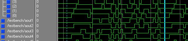
44

45
46 U(x) 10 42
47 43
48 10 r0,r1,r2,r3,r4,r5,r6,r7, r8,r9 44
49 A 45
50
51 4 VHDL LeonardoSpectrum LS2001_1a_31 VHDL Design Wave

52 Transmitter RECEIVER ERRORCNT SB SBWE START START RBWE RBEC 48
53 RBEC START2 START START2 RB RBEC 8 49
54 4.2 TRANSMITTER TRANSMITTER 4.2.1TRANSMITTER TRANSMITTER TRANSMITTER 2.1. TV TV TRANSMITTER TRANSMITTER TRANSMITTER errsig 50

55 START 21 RECEIVER TRANSMITTER 51
56 Phase infbit IN intsb intsb infbit infbit 10 parity 0 1 errsig 33 0 parity(9) intsb2 intsb2 SB errsig SBWE START 21 START 52
57 4.2.4 ALTERA MAX+plus 10.1 BASELINE [2],[3],[4] TRANSMITTER VHDL TRANSMITTER
58 4.2.5VHDL library IEEE; use IEEE.STD_LOGIC_1164.all, IEEE.STD_LOGIC_unsigned.all; entity TRANSMITTER is Port (SBWE: out std_logic; SB : out std_logic; START : out std_logic; RESET : in std_logic; CLK : in std_logic ); end TRANSMITTER; architecture RTL of TRANSMITTER is signal phase : std_logic_vector (5 downto 0); -- phase counts from 0 to phase 0 to 20 : sync bits are transmitted -- phase 21 to 31 : information bits transmitted -- phase 32 to 41 : parity bits transmitted signal infbit : std_logic_vector (10 downto 0); -- 11bits information bits signal intstart : std_logic; -- internal start signal signal intsb,intsb2 : std_logic; -- internal sb signal signal parity : std_logic_vector (9 downto 0); parity bits signal errsig : std_logic; -- error signal signal errcnt : std_logic_vector (9 downto 0); -- error counter begin phase (0 to 41 counter) generation unit PHASE_CNT: process(clk,reset) 54
59 begin if (RESET='1') then phase <= "000000"; elsif rising_edge(clk) then if (phase="101001") then -- if phase=41 phase <= "000000"; else phase <= phase + 1; end if; end if; end process PHASE_CNT; bits information generation unit -- count down from by INF_GEN: process(clk, RESET) begin if (RESET='1') then infbit <= " "; elsif rising_edge(clk) then if (phase="010100") then -- if phase=20 infbit <= infbit - 1; end if; end if; end process INF_GEN; internal start (intstart) generation START_GEN: process(clk, RESET) begin if (RESET='1') then intstart <= '0'; elsif rising_edge(clk) then if (phase="010101") then -- if phase=21 intstart <= '1'; 55
60 else intstart <= '0'; end if; end if; end process START_GEN; internal sb signal (intsb) generation SB_GEN: process(clk, RESET) begin if (RESET='1') then intsb <= '0'; elsif rising_edge(clk) then case phase is when "000000"=> intsb <= '0'; -- 0 when "000001"=> intsb <= '0'; -- 1 when "000010"=> intsb <= '1'; -- 2 when "000011"=> intsb <= '1'; -- 3 when "000100"=> intsb <= '0'; -- 4 when "000101"=> intsb <= '1'; -- 5 when "000110"=> intsb <= '0'; -- 6 when "000111"=> intsb <= '1';-- 7 when "001000"=> intsb <= '1'; -- 8 when "001001"=> intsb <= '1'; -- 9 when "001010"=> intsb <= '1'; --10 when "001011"=> intsb <= '0'; --11 when "001100"=> intsb <= '1'; --12 when "001101"=> intsb <= '1'; --13 when "001110"=> intsb <= '1';--14 when "001111"=> intsb <= '0'; --15 when "010000"=> intsb <= '0'; --16 when "010001"=> intsb <= '0'; --17 when "010010"=> intsb <= '0'; --18 when "010011"=> intsb <= '0'; --19 when "010100"=> intsb <= '0'; --20 when "010101"=> intsb <= infbit(10);
61 when "010110"=> intsb <= infbit(9); --22 when "010111"=> intsb <= infbit(8); --23 when "011000"=> intsb <= infbit(7); --24 when "011001"=> intsb <= infbit(6); --25 when "011010"=> intsb <= infbit(5); --26 when "011011"=> intsb <= infbit(4); --27 when "011100"=> intsb <= infbit(3); --28 when "011101"=> intsb <= infbit(2); --29 when "011110"=> intsb <= infbit(1); --30 when "011111"=> intsb <= infbit(0); --31 when others => intsb <= 'X'; --others end case; end if; end process SB_GEN; parity calculation PARITY_CAL: process(clk, RESET) begin if (RESET='1') then parity <= " "; elsif rising_edge(clk) then if (phase="010101") then parity <= " "; elsif (phase>="010110" and phase<="100000") then parity(9) <= parity(8); parity(8) <= parity(7); parity(7) <= parity(6) xor intsb xor parity(9); parity(6) <= parity(5) xor intsb xor parity(9); parity(5) <= parity(4); parity(4) <= parity(3) xor intsb xor parity(9); parity(3) <= parity(2); parity(2) <= parity(1) xor intsb xor parity(9); parity(1) <= parity(0); 57
62 parity(0) <= intsb xor parity(9); else parity <= parity(8 downto 0) & parity(9); end if; end if; end process PARITY_CAL; error interval counter ERR_CNT: process (CLK, RESET) begin if (RESET='1') then errcnt <= " "; elsif rising_edge(clk) then if (errcnt = " ") then -- max=9 (0-9) errcnt <= " "; else errcnt <= errcnt +1; end if; end if; end process ERR_CNT; error signal generation ERROR_GEN: process (CLK, RESET) begin if (RESET='1') then errsig <= '0'; elsif rising_edge(clk) then if (errcnt=" ") then errsig <= '1';-- error happens every 10 else errsig <= '0'; end if; end if; end process ERROR_GEN; output signals
63 SBOUT: process (CLK, RESET) begin if (RESET='1') then intsb2 <= '0'; elsif rising_edge(clk) then if(phase >="100001" or phase="000000") then intsb2 <= parity(9); else intsb2 <= intsb; end if; end if; end process SBOUT; startout STARTOUT: process (CLK, RESET) begin if (RESET='1') then START <= '0'; elsif rising_edge(clk) then START <= intstart; end if; end process STARTOUT; SB <= intsb2; SBWE <= intsb2 xor errsig; end RTL; 59
64 LIBRARY ieee; USE ieee.std_logic_1164.all; USE ieee.numeric_std.all; ENTITY testbench IS END testbench; ARCHITECTURE behavior OF testbench IS COMPONENT transmitter PORT( RESET : IN std_logic; CLK : IN std_logic; SBWE : OUT std_logic; SB : OUT std_logic; START : OUT std_logic ); END COMPONENT; SIGNAL cycle : integer := 0; SIGNAL SBWE : std_logic; SIGNAL SB : std_logic; SIGNAL START : std_logic; SIGNAL RESET : std_logic:= '1'; SIGNAL CLK : std_logic:= '0'; BEGIN uut: transmitter PORT MAP( SBWE => SBWE, SB => SB, START => START, RESET => RESET, CLK => CLK ); 60
; end loop RESET_LOOP; RESET <= '0'; CAL_LOOP: for N in 0 to 500 loop wait until falling_edge(clk); end loop CAL_LOOP; end process; end architecture behavior; 4.")
65 process begin if (cycle < 300)then cycle <= cycle +1; wait for 10 ns; CLK <= not CLK; else wait; end if; end process; process begin RESET_LOOP: for N IN 0 to 3 loop wait until falling_edge(clk); end loop RESET_LOOP; RESET <= '0'; CAL_LOOP: for N in 0 to 500 loop wait until falling_edge(clk); end loop CAL_LOOP; end process; end architecture behavior; 4.4TRANSMITTER 61
66 4.2.6 LeonardoSpectrum LS2001_1a_ LeonardoSpectrum LS2001_1a_ TRANSMITTER UNIT
67 4.350 XOR Critical path #1, (unconstrained path) NAME GATE ARRIVAL LOAD A(36)/ up 0.08 ix69/x XR2T up 0.08 ix255/x XN3R up 0.14 ix75/x XN2R dn 0.08 ix91/x XN3R up 0.09 ix95/x XR3T up 0.21 ix97/x XR3T up 0.04 Y/ up 0.00 data arrival time 2.99 data required time not specified data required time not specified data arrival time unconstrained path ******************************************************* Cell: xor50inputs View: RTL Library: work ******************************************************* Cell Library References Total Area XN2R0 scl05u 3 x 5 15 gates XN3R0 scl05u 9 x 7 61 gates XR2T0 scl05u 12 x 5 59 gates XR3T0 scl05u 8 x 7 54 gates Number of ports : 51 Number of nets : 82 Number of instances : 32 Number of references to this view : 0 Total accumulated area : Number of gates :
68 64
69 65
70 4.5TRNSMITTER 66
71 4.3 RCEIVER RECEIVER 4.3.1RCEIVER RECEIVER RECEIVER 2.1. TV/ RECEIVER Ensig 1 RBWE START 1 42 N 41 2 Ensig 1 START2 RBEC START2 67

72 , IN TRANSMITTER SBWE= RBWE CLKCLOCK RESETRESET OUT RECEIVER RBWE START2 OUT START2 4.6RECEIVER 68
73 Phase EN ENsig ENsig RBWE 21 INPUT INPUT Esig Parity(9) ER_out S_erc_out S_erc_out 41 0 A1+A2 + A3 + A4 + A5 3 P_out ENsig 0 P_out ER_out 21 INPUT REG_Q(20) ER_out REG_Q(20) RBEC START2 START2 69
74 4.7 70

75 4.3.4 TRANSMITTER ALTERA MAX+plus 10.1 BASELINE
76 4.3.5VHDL library IEEE; use IEEE.STD_LOGIC_1164.all, IEEE.NUMERIC_STD.all; entity RECEIVER is Port ( START : in std_logic; RBWE : in std_logic; START2 : out std_logic; RBEC : out std_logic; RESET : in std_logic; CLK : in std_logic ); end RECEIVER; architecture RTL of RECEIVER is signal INPUT : std_logic; signal ENsig : std_logic; signal phase : unsigned (5 downto 0); signal intstart : std_logic; signal parity : unsigned (9 downto 0); signal REG_Q : unsigned (20 downto 0 ); signal P_out : std_logic; signal ER_out : std_logic; signal S_erc_out : std_logic; signal A1,A2,A3,A4,A5 : std_logic; begin -- RBWE input to the receiver -- ENABLE signal -- phase signals -- internal start signal parity bits -- 21bits sifht register signals -- output signal of majority circuit -- Error correction signal -- Input signal to the error check circuit -- parity check signals 72
77 phase (41 downto 0 counter) generation unit PHASE_CNT1: process(clk,reset) begin if (RESET='1') then phase <= "000000"; elsif rising_edge(clk) then if (START='1')then phase <= "101001"; elsif (phase= "000000")then phase <= "000000"; else phase <= phase -1; end if; end if; end process PHASE_CNT1; ENABLE signal1 generation EN1_GEN: process (START,phase) begin if (phase>="010110" and phase<="101001")then ENsig <='1'; else ENsig <='0'; end if; end process EN1_GEN; Controlled RBWE siganl RB_n: process(clk,ensig) begin if(ensig='1')then INPUT <= RBWE; 73
78 else INPUT <= '0'; end if; end process RB_n; bit SHIFT_REGISTER SFIT_R21: process(clk, RESET) begin if ( RESET = '1') then REG_Q <= ( others => '0'); elsif rising_edge(clk) then REG_Q(0) <= INPUT; REG_Q (20 downto 1) <= REG_Q (19 downto 0); end if; end process; Internal start2 (intstart) generation START_GEN: process(clk, RESET) begin if (RESET='1') then intstart <= '0'; elsif rising_edge(clk) then if (phase="010111") then intstart <= '1'; else intstart <= '0'; end if; end if; end process START_GEN; Input to the error_checker S_erc_out <= (INPUT and ENsig) xor parity(9) xor ER_out; 74
79 Parity_calculation PARITY_CAL: process(clk,reset,phase) begin if (RESET='1') then parity <= " "; elsif rising_edge(clk) then if (phase>="000000" and phase<="101001")then parity(9) <= parity(8); parity(8) <= parity(7); parity(7) <= parity(6) xor parity(9); parity(6) <= parity(5) xor parity(9); parity(5) <= parity(4); parity(4) <= parity(3) xor parity(9); parity(3) <= parity(2); parity(2) <= parity(1) xor parity(9); parity(1) <= parity(0); parity(0) <= S_erc_out; end if; end if; end process PARITY_CAL; Parity input to the parity_checker A1 <= parity(9); A2 <= parity(1); A3 <= parity(4) xor parity(6); A4 <= parity(0) xor parity(5) xor parity(7); A5 <= parity(2) xor parity(3) xor parity(8); Output from the majority circuit PROCESS (A1,A2,A3,A4,A5) BEGIN 75
80 if (A1='1' and A2='1' and A3='1')then P_out <= '1'; elsif (A4='1' and A5='1')then P_out <= A1 or A2 or A3; elsif (A1='1' and A2='1') then P_out <= A4 or A5; elsif (A3='1' and A5='1')then P_out <= A1 or A2; elsif (A3='1' and A4='1')then P_out <= A1 or A2; else P_out <= '0'; end if; end process; Output from signal of ERROR checker ER_out <= P_out and not ENsig; Output signal RBEC <= (REG_Q(20) xor ER_out); Startout STARTOUT2: process (CLK, RESET) begin if (RESET='1') then START2 <= '0'; elsif rising_edge(clk) then START2 <= intstart; end if; end process STARTOUT2; end RTL; 76
81 4.6RECEIVER 1/5 LIBRARY ieee; USE ieee.std_logic_1164.all; USE ieee.numeric_std.all; ENTITY testbench IS END testbench; ARCHITECTURE behavior OF testbench IS COMPONENT receiver PORT( START : IN std_logic; RBWE : IN std_logic; RESET : IN std_logic; CLK : IN std_logic; START2 : OUT std_logic; RBEC : OUT std_logic ); END COMPONENT; SIGNAL cycle : integer := 0; SIGNAL START : std_logic; SIGNAL RBWE : std_logic; SIGNAL START2 : std_logic; SIGNAL RBEC : std_logic; SIGNAL RESET : std_logic:= '1'; SIGNAL CLK : std_logic:= '0'; BEGIN uut: receiver PORT MAP( START => START, RBWE => RBWE, START2 => START2, RBEC => RBEC, RESET => RESET, CLK => CLK ); 77
82 4.6RECEIVER 2/5 process begin if (cycle < 300)then cycle <= cycle +1; wait for 10 ns; CLK <= not CLK; else wait; end if; end process; process begin RESET_LOOP: for N IN 0 to 3 loop wait until falling_edge(clk); end loop RESET_LOOP; RESET <= '0'; CAL_LOOP: for N in 0 to 500 loop wait until falling_edge(clk); end loop CAL_LOOP; end process; process begin RBWE <= '0'; wait for 80 ns; RBWE <= '1'; wait for 20 ns; RBWE <= '0'; wait for 20 ns; RBWE <= '0'; wait for 20 ns; RBWE <= '1'; wait for 20 ns; RBWE <= '1'; wait for 20 ns; RBWE <= '0'; wait for 20 ns; RBWE <= '1'; wait for 20 ns; RBWE <= '0'; wait for 20 ns; RBWE <= '1'; wait for 20 ns; RBWE <= '1'; 78
83 4.6RECEIVER 3/5 wait for 20 ns; RBWE <= '0'; wait for 20 ns; RBWE <= '1'; wait for 20 ns; RBWE <= '0'; wait for 20 ns; RBWE <= '1'; wait for 20 ns; RBWE <= '1'; wait for 20 ns; RBWE <= '1'; wait for 20 ns; RBWE <= '0'; wait for 20 ns; RBWE <= '0'; wait for 20 ns; RBWE <= '0'; wait for 20 ns; RBWE <= '0'; wait for 20 ns; RBWE <= '1'; wait for 20 ns; RBWE <= '0'; wait for 20 ns; RBWE <= '1'; wait for 20 ns; RBWE <= '1'; wait for 20 ns; RBWE <= '1'; wait for 20 ns; RBWE <= '1'; wait for 20 ns; RBWE <= '1'; wait for 20 ns; RBWE <= '1'; wait for 20 ns; RBWE <= '1'; wait for 20 ns; RBWE <= '1'; wait for 20 ns; RBWE <= '0'; wait for 20 ns; RBWE <= '1'; wait for 20 ns; RBWE <= '1'; wait for 20 ns; RBWE <= '0'; wait for 20 ns; RBWE <= '0'; wait for 20 ns; RBWE <= '0'; wait for 20 ns; RBWE <= '1'; wait for 20 ns; RBWE <= '0'; wait for 20 ns; RBWE <= '0'; wait for 20 ns; RBWE <= '1'; wait for 20 ns; RBWE <= '0'; wait for 20 ns; RBWE <= '0'; 79
84 4.6RECEIVER 4/5 wait for 20 ns; RBWE <= '0'; wait for 20 ns; RBWE <= '0'; wait for 20 ns; RBWE <= '0'; wait for 20 ns; RBWE <= '1'; wait for 20 ns; RBWE <= '1'; wait for 20 ns; RBWE <= '0'; wait for 20 ns; RBWE <= '1'; wait for 20 ns; RBWE <= '0'; wait for 20 ns; RBWE <= '1'; wait for 20 ns; RBWE <= '1'; wait for 20 ns; RBWE <= '0'; wait for 20 ns; RBWE <= '1'; wait for 20 ns; RBWE <= '0'; wait for 20 ns; RBWE <= '1'; wait for 20 ns; RBWE <= '1'; wait for 20 ns; RBWE <= '1'; wait for 20 ns; RBWE <= '0'; wait for 20 ns; RBWE <= '0'; wait for 20 ns; RBWE <= '0'; wait for 20 ns; RBWE <= '0'; wait for 20 ns; RBWE <= '1'; wait for 20 ns; RBWE <= '0'; wait for 20 ns; RBWE <= '1'; wait for 20 ns; RBWE <= '1'; wait for 20 ns; RBWE <= '1'; wait for 20 ns; RBWE <= '1'; wait for 20 ns; RBWE <= '1'; wait for 20 ns; RBWE <= '1'; wait for 20 ns; RBWE <= '0'; wait for 20 ns; RBWE <= '1'; wait for 20 ns; RBWE <= '1'; wait for 20 ns; RBWE <= '1'; 80
85 4.6RECEIVER 5/5 wait for 20 ns; RBWE <= '0'; wait for 20 ns; RBWE <= '0'; wait for 20 ns; RBWE <= '0'; wait for 20 ns; RBWE <= '1'; wait for 20 ns; RBWE <= '0'; wait for 20 ns; RBWE <= '0'; wait for 20 ns; RBWE <= '0'; wait for 20 ns; RBWE <= '1'; wait for 20 ns; RBWE <= '0'; wait for 20 ns; RBWE <= '0'; wait for 20 ns; RBWE <= '1'; wait for 20 ns; RBWE <= '0'; wait; end process; process begin START <= '0'; wait for 520 ns; START <= '1'; wait for 20 ns; START <= '0'; wait for 820 ns; START <= '1'; wait for 20 ns; START <= '0'; wait; end process; end architecture behavior; 4.10RECEIVER 81
86 4.3.6 LeonardoSpectrum LS2001_1a_ XOR RECEIVER UNIT RECEIVER 1/3 Critical Path Report Critical path #1, (unconstrained path) NAME GATE ARRIVAL LOAD clock information not specified delay thru clock network 0.00 (ideal) reg_phase(1)/q FD1B dn 0.20 ix579/x NR2R up 0.19 ix47/x ND2N dn 0.27 ix576/x NR2R up 0.19 ix79/x ND2N dn
87 4.7RECEIVER 2/3 ix573/x NR2R up 0.16 ix571/x NR2R dn 0.17 ix11/x AN2T dn 0.11 reg_phase(0)/d FD1B dn 0.00 data arrival time 3.93 data required time not specified data required time not specified data arrival time unconstrained path ****************************************************** Cell: RECEIVER View: RTL Library: work ******************************************************* Cell Library References Total Area AN2T0 scl05u 5 x 5 24 gates AO1A0 scl05u 1 x 6 6 gates AO2L0 scl05u 2 x 8 15 gates AOA4I0 scl05u 1 x 8 8 gates AOA4I2 scl05u 1 x 8 8 gates FD1B0 scl05u 29 x gates FD1I0 scl05u 9 x gates FD1I1 scl05u 1 x gates IV1N0 scl05u 3 x 3 9 gates IV1NP scl05u 2 x 4 8 gates ND2N0 scl05u 5 x 5 23 gates NR2R0 scl05u 4 x 5 18 gates NR3R0 scl05u 1 x 6 6 gates NR4R1 scl05u 1 x 8 8 gates OAI1A0 scl05u 3 x 6 19 gates OAI3R2 scl05u 1 x 8 8 gates 83

88 4.7RECEIVER 3/3 XN2R0 scl05u 10 x 5 49 gates XN3R0 scl05u 3 x 7 20 gates Number of ports : 6 Number of nets : 89 Number of instances : 82 Number of references to this view : 0 Total accumulated area : Number of gates : RECEIVER 84
89 VHDL TRANSMITTER RECEINVER ERRORCNT 85
90
91
92
93 89
94 90
95
96
97 VHDL FPGA DesignWave
98 94
99 [8] Design Wave Magagin CQ [9] Design Wave Magagin CQ [10] NHK informationhttp:// [11] FM [12] ON-LINE Bit Bit Bit 95
if clear = 1 then Q <= " "; elsif we = 1 then Q <= D; end rtl; regs.vhdl clk 0 1 rst clear we Write Enable we 1 we 0 if clk 1 Q if rst =
 VHDL 2 1 VHDL 1 VHDL FPGA VHDL 2 HDL VHDL 2.1 D 1 library ieee; use ieee.std_logic_1164.all; use ieee.std_logic_unsigned.all; regs.vhdl entity regs is clk, rst : in std_logic; clear : in std_logic; we
1 1 2 2 2-1 2 2-2 4 2-3 11 2-4 12 2-5 14 3 16 3-1 16 3-2 18 3-3 22 4 35 4-1 VHDL 35 4-2 VHDL 37 4-3 VHDL 37 4-3-1 37 4-3-2 42 i
 1030195 15 2 10 1 1 2 2 2-1 2 2-2 4 2-3 11 2-4 12 2-5 14 3 16 3-1 16 3-2 18 3-3 22 4 35 4-1 VHDL 35 4-2 VHDL 37 4-3 VHDL 37 4-3-1 37 4-3-2 42 i 4-3-3 47 5 52 53 54 55 ii 1 VHDL IC VHDL 5 2 3 IC 4 5 1 2
VHDL
 VHDL 1030192 15 2 10 1 1 2 2 2.1 2 2.2 5 2.3 11 2.3.1 12 2.3.2 12 2.4 12 2.4.1 12 2.4.2 13 2.5 13 2.5.1 13 2.5.2 14 2.6 15 2.6.1 15 2.6.2 16 3 IC 17 3.1 IC 17 3.2 T T L 17 3.3 C M O S 20 3.4 21 i 3.5 21
スライド 1
 1 1. 2 2. 3 isplever 4 5 6 7 8 9 VHDL 10 VHDL 4 Decode cnt = "1010" High Low DOUT CLK 25MHz 50MHz clk_inst Cnt[3:0] RST 2 4 1010 11 library ieee; library xp; use xp.components.all; use ieee.std_logic_1164.all;
論理設計の基礎
 . ( ) IC (Programmable Logic Device, PLD) VHDL 2. IC PLD 2.. PLD PLD PLD SIC PLD PLD CPLD(Complex PLD) FPG(Field Programmable Gate rray) 2.2. PLD PLD PLD I/O I/O : PLD D PLD Cp D / Q 3. VHDL 3.. HDL (Hardware
TECH_I Vol.25 改訂新版PCIデバイス設計入門
 library ieee; use ieee.std_logic_1164.all; use ieee.std_logic_unsigned.all; entity n is port( ); end entity n; architecture RTL of nis begin when : process begin end process :process begin end process
Unconventional HDL Programming ( version) 1
 1") Unconventional HDL Programming (20090425 version) 1 1 Introduction HDL HDL Hadware Description Language printf printf (C ) HDL 1 HDL HDL HDL HDL HDL HDL 1 2 2 2.1 VHDL 1 library ieee; 2 use ieee.std_logic_1164.all;
Unconventional HDL Programming (20090425 version) 1 1 Introduction HDL HDL Hadware Description Language printf printf (C ) HDL 1 HDL HDL HDL HDL HDL HDL 1 2 2 2.1 VHDL 1 library ieee; 2 use ieee.std_logic_1164.all;
------------------------------------------------------------------------------------------------------- 1 --------------------------------------------
 ------------------------------------------------------------------------------------------------------- 1 -------------------------------------------------------------------------- 2 -----------------------------------------------------------------------------
Microsoft PowerPoint LC_15.ppt
 ( 第 15 回 ) 鹿間信介摂南大学理工学部電気電子工学科 特別講義 : 言語を使った設計 (2) 2.1 HDL 設計入門 2.2 FPGA ボードの設計デモ配布資料 VHDL の言語構造と基本文法 2.1 HDL 設計入門 EDAツール : メンター社製品が有名 FPGAベンダーのSW 1 1 仕様設計 にも簡易機能あり 2 3 2 HDLコード記述 3 論理シミュレーション 4 4 論理合成
Microsoft Word - 実験4_FPGA実験2_2015
 FPGA の実験 Ⅱ 1. 目的 (1)FPGA を用いて組合せ回路や順序回路を設計する方法を理解する (2) スイッチや表示器の動作を理解し 入出力信号を正しく扱う 2. スケジュール項目 FPGAの実験 Ⅱ( その1) FPGAの実験 Ⅱ( その2) FPGAの実験 Ⅱ( その3) FPGAの実験 Ⅱ( その4) FPGAの実験 Ⅱ( その5) FPGAの実験 Ⅱ( その6) FPGAの実験 Ⅱ(
スライド 1
 isplever CLASIC 1.2 Startup Manual for MACH4000 Rev.1.0 isplever_ CLASIC Startup_for_MACH4000_Rev01.ppt Page: 1 1. Page 3 2. Lattice isplever Design Flow Page 4 3. Page 5 3-1 Page 6 3-2 Page 7 3-3 Page
Microsoft PowerPoint - 集積回路工学_ ppt[読み取り専用]
![Microsoft PowerPoint - 集積回路工学_ ppt[読み取り専用]](/thumbs/88/116763841.jpg "Microsoft PowerPoint - 集積回路工学_ ppt[読み取り専用]") 2007.11.12 集積回路工学 Matsuzawa Lab 1 集積回路工学 東京工業大学 大学院理工学研究科 電子物理工学専攻 2007.11.12 集積回路工学 Matsuzawa Lab 2 1. 1. ハードウェア記述言語 (VHDL で回路を設計 ) HDL 設計の手順や基本用語を学ぶ RTL とは? Register Transfer Level レジスタ間の転送関係を表現したレベル慣例的に以下のことを行う
2007.11.12 集積回路工学 Matsuzawa Lab 1 集積回路工学 東京工業大学 大学院理工学研究科 電子物理工学専攻 2007.11.12 集積回路工学 Matsuzawa Lab 2 1. 1. ハードウェア記述言語 (VHDL で回路を設計 ) HDL 設計の手順や基本用語を学ぶ RTL とは? Register Transfer Level レジスタ間の転送関係を表現したレベル慣例的に以下のことを行う
エンティティ : インタフェースを定義 entity HLFDD is port (, : in std_logic ;, : out std_logic ) ; end HLFDD ; アーキテクチャ : エンティティの実現 architecture RH1 of HLFDD is <= xor
 ; end HLFDD ; アーキテクチャ : エンティティの実現 architecture RH1 of HLFDD is <= xor") VHDL を使った PLD 設計のすすめ PLD 利用のメリット 小型化 高集積化 回路の修正が容易 VHDL 設計のメリット 汎用の設計になる ( どこのデバイスにも搭載可能 ) 1/16 2001/7/13 大久保弘崇 http://www.aichi-pu.ac.jp/ist/~ohkubo/ 2/16 設計の再利用が促進 MIL 記号の D での設計との比較 Verilog-HDL などでも別に同じ
VHDL を使った PLD 設計のすすめ PLD 利用のメリット 小型化 高集積化 回路の修正が容易 VHDL 設計のメリット 汎用の設計になる ( どこのデバイスにも搭載可能 ) 1/16 2001/7/13 大久保弘崇 http://www.aichi-pu.ac.jp/ist/~ohkubo/ 2/16 設計の再利用が促進 MIL 記号の D での設計との比較 Verilog-HDL などでも別に同じ
フリップフロップ
 第 3 章フリップ フロップ 大阪大学大学院情報科学研究科 今井正治 imai@ist.osaka-u.ac.jp http://www-ise1.ist.osaka-u.ac.jp/~imai/ 2005/10/17 2006, Masaharu Imai 1 講義内容 フリップ フロップの基本原理 RS フリップ フロップ D ラッチ D フリップ フロップ JK フリップ フロップ T フリップ
問 2. タイミングチャート以下に示す VHDL コードで記述されている回路に関するタイミングチャートを完成させよ ) レジスタの動作 use IEEE.std_logic_64.all; entity RegN is generic (N : integer := 8 port ( CLK, EN
 レジスタの動作 use IEEE.std_logic_64.all; entity RegN is generic (N : integer := 8 port ( CLK, EN") 第 8 回中間試験前の演習 問.VHDL ソースコードを読む () 次の VHDL のソースコードが記述しているゲート回路の回路図を示せ. use IEEE.STD_LOGIC_64.ALL; use IEEE.STD_LOGIC_ARITH.ALL; use IEEE.STD_LOGIC_UNSIGNED.ALL; entity Logic is port ( A : in std_logic_vector(3
第 8 回中間試験前の演習 問.VHDL ソースコードを読む () 次の VHDL のソースコードが記述しているゲート回路の回路図を示せ. use IEEE.STD_LOGIC_64.ALL; use IEEE.STD_LOGIC_ARITH.ALL; use IEEE.STD_LOGIC_UNSIGNED.ALL; entity Logic is port ( A : in std_logic_vector(3
PeakVHDL Max+Plus VGA VG
 2001 PC 9720002 14 2 7 4 1 5 1.1... 5 1.2... 5 1.3... 6 1.4... 6 2 7 2.1... 7 2.2... 8 2.2.1... 8 2.3... 9 2.3.1 PeakVHDL... 9 2.3.2 Max+Plus2... 9 3 VGA 10 3.1... 10 3.2 VGA... 10 3.3 VGA... 11 3.4 VGA...
デザインパフォーマンス向上のためのHDLコーディング法
 WP231 (1.1) 2006 1 6 HDL FPGA TL TL 100MHz 400MHz HDL FPGA FPGA 2005 2006 Xilinx, Inc. All rights reserved. XILINX, the Xilinx logo, and other designated brands included herein are trademarks of Xilinx,
卒 業 研 究 報 告
 VHDL 1040183 16 2 17 1 1 2 2 2 2 2 1 2 2 2 3 7 3 18 19 20 22 23 25 4 VHDL 27 27 8 BCD 2 27 28 REG_B 29 29 STATE 29 31 VHDL 5 VHDL 1 CPU Hardware Description Language : HDL VHDL VHSIC HDL 1 2 3 VHDL 4 3
- VHDL 演習 ( 組み合せ論理回路 ) 回路 半加算器 (half adder,fig.-) 全加算器を構成する要素である半加算器を作成する i) リスト - のコードを理解してから, コンパイル, ダウンロードする ii) 実験基板上のスイッチ W, が, の入力,LED, が, の出力とな
 回路 半加算器 (half adder,fig.-) 全加算器を構成する要素である半加算器を作成する i) リスト - のコードを理解してから, コンパイル, ダウンロードする ii) 実験基板上のスイッチ W, が, の入力,LED, が, の出力とな") 第 回 VHDL 演習組み合せ論理回路 VHDL に関する演習を行う 今回は, 組み合せ論理回路の記述について学ぶ - 論理回路の VHDL 記述の基本 同時処理文を並べることで記述できる 部品の接続関係を記述 順番は関係ない process 文の内部では, 順次処理文を使う process 文 つで, つの同時処理文になる順次処理文は, 回路の動作を 逐次処理的 に ( 手続き処理型プログラム言語のように
第 回 VHDL 演習組み合せ論理回路 VHDL に関する演習を行う 今回は, 組み合せ論理回路の記述について学ぶ - 論理回路の VHDL 記述の基本 同時処理文を並べることで記述できる 部品の接続関係を記述 順番は関係ない process 文の内部では, 順次処理文を使う process 文 つで, つの同時処理文になる順次処理文は, 回路の動作を 逐次処理的 に ( 手続き処理型プログラム言語のように
RSA FA FA AND Booth FA FA RSA 3 4 5
 RSA High-Speed Multiplication for RSA ode using Redundant Binary System 6585 6 6 RSA FA FA AND Booth FA FA RSA 3 4 5 This paper summarizes High-Speed Multiplication for RSA ode using Redundant Binary System,
回路 7 レジスタ ( 同期イネーブル及び非同期リセット付 ) 入力データを保持するのに用いる記憶素子 使用用途として, マイクロプロセッサ内部で演算や実行状態の保持に用いられる Fig4-2 のレジスタは, クロック信号の立ち上がり時かつ 信号が 1 のときに外部からの 1 ビットデータ R をレ
 入力データを保持するのに用いる記憶素子 使用用途として, マイクロプロセッサ内部で演算や実行状態の保持に用いられる Fig4-2 のレジスタは, クロック信号の立ち上がり時かつ 信号が 1 のときに外部からの 1 ビットデータ R をレ") 第 4 回 VHDL 演習 2 プロセス文とステートマシン プロセス文を用いるステートマシンの記述について学ぶ 回路 6 バイナリカウンタ (Fig.4-1) バイナリカウンタを設計し, クロック信号に同期して動作する同期式回路の動作を学ぶ ⅰ) リスト 4-1 のコードを理解してから, コンパイル, ダウンロードする ⅱ) 実験基板上のディップスイッチを用いて, 発生するクロック周波数を 1Hz
第 4 回 VHDL 演習 2 プロセス文とステートマシン プロセス文を用いるステートマシンの記述について学ぶ 回路 6 バイナリカウンタ (Fig.4-1) バイナリカウンタを設計し, クロック信号に同期して動作する同期式回路の動作を学ぶ ⅰ) リスト 4-1 のコードを理解してから, コンパイル, ダウンロードする ⅱ) 実験基板上のディップスイッチを用いて, 発生するクロック周波数を 1Hz
Design at a higher level
 Meropa FAST 97 98 10 HLS, Mapping, Timing, HDL, GUI, Chip design Cadence, Synopsys, Sente, Triquest Ericsson, LSI Logic 1980 RTL RTL gates Applicability of design methodologies given constant size of
Verilog HDL による回路設計記述
 Verilog HDL 3 2019 4 1 / 24 ( ) (RTL) (HDL) RTL HDL アルゴリズム 動作合成 論理合成 論理回路 配置 配線 ハードウェア記述言語 シミュレーション レイアウト 2 / 24 HDL VHDL: IEEE Std 1076-1987 Ada IEEE Std 1164-1991 Verilog HDL: 1984 IEEE Std 1364-1995
Stratix IIIデバイスの外部メモリ・インタフェース
 8. Stratix III SIII51008-1.1 Stratix III I/O R3 SRAM R2 SRAM R SRAM RII+ SRAM RII SRAM RLRAM II 400 MHz R Stratix III I/O On-Chip Termination OCT / HR 4 36 R ouble ata RateStratix III FPGA Stratix III
main.dvi
 CAD 2001 12 1 1, Verilog-HDL, Verilog-HDL. Verilog-HDL,, FPGA,, HDL,. 1.1, 1. (a) (b) (c) FPGA (d). 2. 10,, Verilog-HDL, FPGA,. 1.2,,,, html. % netscape ref0177/html/index.html.,, View Encoding Japanese
m 1 AUV 10 m 1.3 m 1.5 m 10 tons 300 km 3,500 m 3 kn. Maximum 4 kn SSBL (, ) AUV 2,000 3,
 AUV 2,000 3,") 19 pp.7-17 2006 Development of Deep Sea Cruising Autonomous Underwater Vehicle Taro Aoki Abstract The URASHIMA, a third-generation AUV (Autonomous Underwater Vehicle), can dive to a depth of 3,500 meters,
19 pp.7-17 2006 Development of Deep Sea Cruising Autonomous Underwater Vehicle Taro Aoki Abstract The URASHIMA, a third-generation AUV (Autonomous Underwater Vehicle), can dive to a depth of 3,500 meters,
FPGA と LUPO その1
 FPGA Lecture for LUPO and GTO Vol. 1 2010, 31 August (revised 2013, 19 November) H. Baba Contents FPGA の概要 LUPO の基本的な使い方 New Project Read and Write 基本的な Behavioral VHDL simulation Firmware のダウンロード FPGA
HardCopy IIIデバイスの外部メモリ・インタフェース
 7. HardCopy III HIII51007-1.0 Stratix III I/O HardCopy III I/O R3 R2 R SRAM RII+ RII SRAM RLRAM II R HardCopy III Stratix III LL elay- Locked Loop PLL Phase-Locked Loop On-Chip Termination HR 4 36 HardCopy
PRECISION COMPACT DISC PLAYER DP-75V
 PRECISION COMPACT DISC PLAYER DP-75V Accuphase warranty is valid only in Japan. 7 6 8 9 10 1 2 3 5 4 11 13 14 15 12 16 = CD/PROC PLAY PROGRAM REPEAT ALLONE A B LEVEL khz INDEX TRACK EXT M S db PROCESSOR
2ALU 以下はデータ幅 4ビットの ALU の例 加算, 減算,AND,OR の4つの演算を実行する 実際のプロセッサの ALU は, もっと多種類の演算が可能 リスト 7-2 ALU の VHDL 記述 M use IEEE.STD_LOGIC_1164.ALL; 00 : 加算 use IEE
 差し替え版 第 7 回マイクロプロセッサの VHDL 記述 マイクロプロセッサ全体および主要な内部ユニットの,VHDL 記述の例を示す. 1)MPU(Micro Processor Uit) Module 1MPU のエンティティ記述とコントローラの例以下は, 簡単な MPU の VHDL 記述の例である ただし, アーキテクチャ部分は, 命令読み込みと実行の状態遷移のみを実現したステートマシンである
VHDL
 VHDL 4 4 3 3 6 6 6 9 4 8 5 9 5 5 6 9 3 3 3 35 36 37 38 FIRIIR A/D D/A NOSCOS LSI FIR IIR x a x a a ; ; H a H T j e T j e T j T a j T a T j T a e a H e H T j sin cos sin cos T j I T j R T a e H T a e H
3 SIMPLE ver 3.2: SIMPLE (SIxteen-bit MicroProcessor for Laboratory Experiment) 1 16 SIMPLE SIMPLE 2 SIMPLE 2.1 SIMPLE (main memo
 1 16 SIMPLE SIMPLE 2 SIMPLE 2.1 SIMPLE (main memo") 3 SIMPLE ver 3.2: 20190404 1 3 SIMPLE (SIxteen-bit MicroProcessor for Laboratory Experiment) 1 16 SIMPLE SIMPLE 2 SIMPLE 2.1 SIMPLE 1 16 16 (main memory) 16 64KW a (C )*(a) (register) 8 r[0], r[1],...,
3 SIMPLE ver 3.2: 20190404 1 3 SIMPLE (SIxteen-bit MicroProcessor for Laboratory Experiment) 1 16 SIMPLE SIMPLE 2 SIMPLE 2.1 SIMPLE 1 16 16 (main memory) 16 64KW a (C )*(a) (register) 8 r[0], r[1],...,
BS・110度CSデジタルハイビジョンチューナー P-TU1000JS取扱説明書
 C S0 CS Digital Hi-Vision Tuner C C C C S0-0A TQZW99 0 C C C C 4 5 6 7 8 9 C C C C C C C C C C C C C C C C C C C C C C C 0 FGIH C 0 FGIH C C C FGIH FG IH FGIH I H FGIH FGIH 0 C C # $ IH F G 0 # $ # $
untitled
 13 Verilog HDL 16 CPU CPU IP 16 1023 2 reg[ msb: lsb] [ ]; reg [15:0] MEM [0:1023]; //16 1024 16 1 16 2 FF 1 address 8 64 `resetall `timescale 1ns/10ps module mem8(address, readdata,writedata, write, read);
<4D F736F F D2091B28BC68CA48B8695F18D902E646F63>
 卒業研究報告 題目 LED ディスプレイ用動画表示制御回路の設計と製作 指導教員 矢野政顕教授 報告者学籍番号 : 1060237 氏名 : 田中振宇 平成 18 年 2 月 21 日 高知工科大学電子 光システム工学科 目次 第 1 章はじめに 1 第 2 章 LED ディスプレイ 2 2-1 LED(Light Emitting Diode) 2 2-1-1 LED の発光原理 2 2-1-2
Cyclone IIIデバイスのI/O機能
 7. Cyclone III I/O CIII51003-1.0 2 Cyclone III I/O 1 I/O 1 I/O Cyclone III I/O FPGA I/O I/O On-Chip Termination OCT Quartus II I/O Cyclone III I/O Cyclone III LAB I/O IOE I/O I/O IOE I/O 5 Cyclone III
HardCopy IIデバイスのタイミング制約
 7. HardCopy II H51028-2.1 Stratix II FPGA FPGA ASIC HardCopy II ASIC NRE Quartus II HardCopy Design Center HCDC Quartus II TimeQuest HardCopy II 2 DR2 TimeQuest TimeQuest FPGA ASIC FPGA ASIC Quartus II
ADC121S Bit, ksps, Diff Input, Micro Pwr Sampling ADC (jp)
") ADC121S625 ADC121S625 12-Bit, 50 ksps to 200 ksps, Differential Input, Micro Power Sampling A/D Converter Literature Number: JAJSAB8 ADC121S625 12 50kSPS 200kSPS A/D ADC121S625 50kSPS 200kSPS 12 A/D 500mV
ADC121S625 ADC121S625 12-Bit, 50 ksps to 200 ksps, Differential Input, Micro Power Sampling A/D Converter Literature Number: JAJSAB8 ADC121S625 12 50kSPS 200kSPS A/D ADC121S625 50kSPS 200kSPS 12 A/D 500mV
プロセッサ・アーキテクチャ
 2. NII51002-8.0.0 Nios II Nios II Nios II 2-3 2-4 2-4 2-6 2-7 2-9 I/O 2-18 JTAG Nios II ISA ISA Nios II Nios II Nios II 2 1 Nios II Altera Corporation 2 1 2 1. Nios II Nios II Processor Core JTAG interface
Compatibility list: vTESTstudio/CANoe
 1.0 および 1.1 で作成されたテストユニットは テスト内で使用されるコマンドに関わらず 必ず下記の最小バージョン以降の CANoe にて実行してください vteststudio 2.0 以上で作成されたテストユニット ( 新機能を使用していない場合 ) は それぞれに応じた最小バージョン以降の CANoe にて実行してください 下記の表にて 各バージョンに対応する要件をご確認ください vteststudio
MAX IIデバイスのIEEE (JTAG)バウンダリ・スキャン・テスト
バウンダリ・スキャン・テスト") 3. MAX II IEEE 49. JTAG MII54-.6 PCB PCB Bed-of-nails PCB 98 Joint Test Action Group JTAG IEEE Std. 49. BST PCB BST 3 3. IEEE Std. 49. Serial Data In Boundary-Scan Cell IC Pin Signal Serial Data Out Core
3. MAX II IEEE 49. JTAG MII54-.6 PCB PCB Bed-of-nails PCB 98 Joint Test Action Group JTAG IEEE Std. 49. BST PCB BST 3 3. IEEE Std. 49. Serial Data In Boundary-Scan Cell IC Pin Signal Serial Data Out Core
企業考動報告書2010 JR西日本 CSRレポート
 H17.9 H17.11 H18.3 H19.2 H19.6H18.10H17.5 H17.6 H18.3 H17.5 H17.6 H17.9 H18.1 H17.10 H18.3 H18.4 H18.7 H19.4 H19.6 H18.10 H18.10. 4 H 17. 25 H19.10H20.10 H21.9 H21.10H22.3H20.10H21.9H20.4 H20.5 H21.4 H21.10
2
 WV-CS570 2 3 4 5 6 7 8 9 10 11 12 13 q w q e 14 1 2 15 3 4 5 16 6 7 8 9 17 1 2 3 18 19 1 2 * RS485 SET UP * UNIT NUMBER SUB ADDRESS BAUD RATE DATA BIT PARITY CHECK STOP BIT X/X WAIT TIME ALARM DATA DELAY
2007-Kanai-paper.dvi
 19 Estimation of Sound Source Zone using The Arrival Time Interval 1080351 2008 3 7 S/N 2 2 2 i Abstract Estimation of Sound Source Zone using The Arrival Time Interval Koichiro Kanai The microphone array
2
 L C -24K 9 L C -22K 9 2 3 4 5 6 7 8 9 10 11 12 11 03 AM 04 05 0 PM 1 06 1 PM 07 00 00 08 2 PM 00 4 PM 011 011 021 041 061 081 051 071 1 2 4 6 8 5 7 00 00 00 00 00 00 00 00 30 00 09 00 15 10 3 PM 45 00
FC741E2_091201
 T101-1587-04 1 2 2 0 0 9 2 0 0 8 0 9 0 1 0 5 0 9 1 4 0 5 1 0 5 5 1 2 3 4 4 5 6 7 8 9 1 2 3 0 3 3 0 2 1 1 5 0 1 3 3 3 0 2 0 3 0 3 4 0 9 1 1 0 9 0 9 1 1 5
Цифровой спутниковый ресивер Lumax DV 2400 IRD
 13... 3 1.... 5 1.1 1.2... 5... 6 2.... 7 2.1 2.2 2.3... 7... 8... 9 3.... 10 3.1... 10 3.1.1 RF...10 3.1.2 SCART...11 3.2... 12 3.2.1 DISH IN...12 3.2.2 DiSEqC...13 4..... 14 4.1 0003.... 15 4.1.1...15
2
 65 2 21 4 1 21 9 30 2 474,973 11.3% 1,060,000 3.1% 8,756 56.8% 24,000 12.1% 8,520 5,405 25.1% 16.5% 18,000 10,000 186.3% 503.5% 3 2.4% 11,344 8.4% 39,908 3.0% 13,932 474,973 14.0% 66,636 19.5% 92,655 52.7%
Keysight MIMO MIMO Cluster n Path n σ n, AoA σ n, AoD Θ n, AoA MS/UE Array Boresight Rx0 Tx0 Θ n, AoD LOS BS Array Boresight Θ n+1, AoA Rx1 Tx1 Path n
 Keysight MIMO MIMO Cluster n Path n σ n, AoA σ n, AoD Θ n, AoA MS/UE Array Boresight Rx0 Tx0 Θ n, AoD LOS BS Array Boresight Θ n+1, AoA Rx1 Tx1 Path n+1 Cluster n+1 ... 3 1. MIMO... 3 1.1 MIMO 1.2 MIMO
0 C C C C C C
 C TU-HD50 TUNER TU - HD50 0 TU-HD50 C C C C S00-06C D D D 0 C C C C 4 5 6 7 8 9 C C C C C C C C C C C C C C C C C C C C C C TUNER TU - HD50 FGIH 0 C C C 0 FGIH C C C C C C FGIH FG IH FGIH I H FGIH FGIH
25 II :30 16:00 (1),. Do not open this problem booklet until the start of the examination is announced. (2) 3.. Answer the following 3 proble
,. Do not open this problem booklet until the start of the examination is announced. (2) 3.. Answer the following 3 proble") 25 II 25 2 6 13:30 16:00 (1),. Do not open this problem boolet until the start of the examination is announced. (2) 3.. Answer the following 3 problems. Use the designated answer sheet for each problem.
25 II 25 2 6 13:30 16:00 (1),. Do not open this problem boolet until the start of the examination is announced. (2) 3.. Answer the following 3 problems. Use the designated answer sheet for each problem.
C FGIH C C C C C C C C C C C C C C C C C C C C C C C C C C C C C C C C C C C C C C C C C C C C C C C C C C C C C C C
 TUDSR5SET TUDSR5 C 7 8 9 ch DIGITAL CS TUNER C C C C S-A C FGIH C C C C C C C C C C C C C C C C C C C C C C C C C C C C C C C C C C C C C C C C C C C C C C C C C C C C C C C C C C C C C C C C C C C C C
OPA134/2134/4134('98.03)
") OPA OPA OPA OPA OPA OPA OPA OPA OPA TM µ Ω ± ± ± ± + OPA OPA OPA Offset Trim Offset Trim Out A V+ Out A Out D In +In V+ Output In A +In A A B Out B In B In A +In A A D In D +In D V NC V +In B V+ V +In
OPA OPA OPA OPA OPA OPA OPA OPA OPA TM µ Ω ± ± ± ± + OPA OPA OPA Offset Trim Offset Trim Out A V+ Out A Out D In +In V+ Output In A +In A A B Out B In B In A +In A A D In D +In D V NC V +In B V+ V +In
PLDとFPGA
 PLDFPGA 2002/12 PLDFPGA PLD:Programmable Logic Device FPGA:Field Programmable Gate Array Field: Gate Array: LSI MPGA:Mask Programmable Gate Array» FPGA:»» 2 FPGA FPGALSI FPGA FPGA Altera, Xilinx FPGA DVD
R1RW0408D シリーズ
 お客様各位 カタログ等資料中の旧社名の扱いについて 2010 年 4 月 1 日を以って NEC エレクトロニクス株式会社及び株式会社ルネサステクノロジが合併し 両社の全ての事業が当社に承継されております 従いまして 本資料中には旧社名での表記が残っておりますが 当社の資料として有効ですので ご理解の程宜しくお願い申し上げます ルネサスエレクトロニクスホームページ (http://www.renesas.com)
<参考>
 B-ISDN User-Network Interface - Physical Layer Specification for 25600kbit/s 1.1 2002 3 1 THE TELECOMMUNICATION TECHNOLOGY COMMITTEE ... 3... 4 1.1... 4 1.2... 4 kbit/s... 4 2.1... 4 2.1.1... 4 2.1.2...
Plastic Package (Note 12) Note 1: ( ) Top View Order Number T or TF See NS Package Number TA11B for Staggered Lead Non-Isolated Package or TF11B for S
 Note 1: ( ) Top View Order Number T or TF See NS Package Number TA11B for Staggered Lead Non-Isolated Package or TF11B for S") Overture 68W ( ) 0.1 (THD N) 20Hz 20kHz 4 68W 8 38W SPiKe (Self Peak Instantaneous Temperature ( Ke)) SOA (Safe Operating Area) SPiKe 2.0 V ( ) 92dB (min) SN 0.03 THD N IMD (SMTPE) 0.004 V CC 28V 4 68W
Overture 68W ( ) 0.1 (THD N) 20Hz 20kHz 4 68W 8 38W SPiKe (Self Peak Instantaneous Temperature ( Ke)) SOA (Safe Operating Area) SPiKe 2.0 V ( ) 92dB (min) SN 0.03 THD N IMD (SMTPE) 0.004 V CC 28V 4 68W
DL1010.PDF
 Delta 1010 24 Bit/96 khz PCI Digital I/O Card 2 M-AUDIO 3 Rack Unit 1. Power LED LED MIDI LED LED MIDI Delta 1010 MIDI MIDI LED LED MIDI Delta 1010 MIDI MIDI MIDI MIDI MIDI MTC Delta 1010 MIDI MIDI MIDI
推奨されるHDLコーディング構文
 6. HDL QII51007-6.0.0 HDL HDL HDL HDL HDL Quartus II Volume 1 Design Recommendations for Altera Devices Quartus II EDA HDL Quartus II Volume 1 Altera Corporation 6 1 Quartus II Volume 1 LPM DSP LVDS PLL
TULを用いたVisual ScalerとTDCの開発
 TUL を用いた Visual Scaler と TDC の開発 2009/3/23 原子核物理 4 年 永尾翔 目次 目的と内容 開発環境 J-Lab におけるハイパー核分光 Visual Scaler TDC まとめ & 今後 目的と内容 目的 TUL, QuartusⅡ を用いて実験におけるトリガーを組めるようになる Digital Logic を組んでみる 内容 特徴 TUL,QuartusⅡ
memo ii
 memo ii iii iv 1 2 3 4 5 6 7 8 1. 2. memo 10 11 12 13 14 15 16 17 18 19 20 21 22 23 24 25 26 27 28 29 30 31 32 33 34 35 36 37 38 39 40 41 42 43 44 45 46 1 2 3 47 1 2 3 48 memo 49 50 51 memo 52 memo 54
2
 WV-CW960 2 3 4 5 6 7 8 9 10 11 SW1 S TA RT RS485Setting SW2 DIP SW1 ON 1 2 3 4 5 6 7 8 ON 1 2 3 4 DIP SW2 12 13 q w q e 14 15 16 17 18 19 ** RS485 SETUP ** UNIT NUMBER SUB ADDRESS BAUD RATE DATA BIT PARITY
「FPGAを用いたプロセッサ検証システムの製作」
 FPGA 2210010149-5 2005 2 21 RISC Verilog-HDL FPGA (celoxica RC100 ) LSI LSI HDL CAD HDL 3 HDL FPGA MPU i 1. 1 2. 3 2.1 HDL FPGA 3 2.2 5 2.3 6 2.3.1 FPGA 6 2.3.2 Flash Memory 6 2.3.3 Flash Memory 7 2.3.4
スライド タイトルなし
 (LNA) (LNA) (PA) ASK FSK PSK BER Bit Error Rate/ratio QPSK GMSK QAM OFDM ASK FSK PSK ASK(Amplitude-shift keying) e( t) = S( t)cos( ω t + θ ) c AM S(t) [+1,0] [+1/2, 1/2] 1 1 2 S(t) 0 1 2 e(t) C O B A E
COINS 5 2.1
 COINS (0501699) 20 21 2 5 1 3 1.1....................................... 3 1.2..................................... 4 1.3....................................... 4 2 COINS 5 2.1 COINS..................................
AN 100: ISPを使用するためのガイドライン
 ISP AN 100: In-System Programmability Guidelines 1998 8 ver.1.01 Application Note 100 ISP Altera Corporation Page 1 A-AN-100-01.01/J VCCINT VCCINT VCCINT Page 2 Altera Corporation IEEE Std. 1149.1 TCK
2
 WV-CW970 2 3 4 5 6 7 8 9 10 11 12 DIP SW1 ON 1 2 3 4 5 6 7 8 ON 1 2 3 4 DIP SW2 SW1 S TA RT RS485Setting SW2 13 14 q w q e 15 16 17 18 19 20 ** RS485 SETUP ** UNIT NUMBER SUB ADDRESS BAUD RATE DATA BIT
LSI LSI 2
 LSI LSI 2 P=CV 2 F 3 4 5 EDA Electric Design Automation) LSI CAD Computer Aided Design) Verilog Verify Logic VHDL VHSIC Description Language) SystemC C SFL Structured Functional description Language) NTT
 ? FPGA FPGA FPGA : : : ? ( ) (FFT) ( ) (Localization) ? : 0. 1 2 3 0. 4 5 6 7 3 8 6 1 5 4 9 2 0. 0 5 6 0 8 8 ( ) ? : LU Ax = b LU : Ax = 211 410 221 x 1 x 2 x 3 = 1 0 0 21 1 2 1 0 0 1 2 x = LUx = b 1 31
untitled
 Verilog HDL Verilog HDL VerilogHDL veriloghdl / CPLD , 1bit 2 MUX 5 D,E) always) module MUX(out, a, b, sel); output out; input a, b, sel; A) IF module MUX(out, a, b, sel); output out; input a, b, sel;

strtok-count.eps
 IoT FPGA 2016/12/1 IoT FPGA 200MHz 32 ASCII PCI Express FPGA OpenCL (Volvox) Volvox CPU 10 1 IoT (Internet of Things) 2020 208 [1] IoT IoT HTTP JSON ( Python Ruby) IoT IoT IoT (Hadoop [2] ) AI (Artificial
R1RP0416D シリーズ
 お客様各位 カタログ等資料中の旧社名の扱いについて 2010 年 4 月 1 日を以って NEC エレクトロニクス株式会社及び株式会社ルネサステクノロジが合併し 両社の全ての事業が当社に承継されております 従いまして 本資料中には旧社名での表記が残っておりますが 当社の資料として有効ですので ご理解の程宜しくお願い申し上げます ルネサスエレクトロニクスホームページ (http://www.renesas.com)
ppt
 / 5 1 (error control) (flow control) / 5 2 Layer 1 gateway: repeater ( ) Layer 2 gateway: bridge ( ) Layer 3 gateway: router (datalink frame) / 5 3 Data link control (error detection / correction) (flow
5 2 5 Stratix IV PLL 2 CMU PLL 1 ALTGX MegaWizard Plug-In Manager Reconfig Alt PLL CMU PLL Channel and TX PLL select/reconfig CMU PLL reconfiguration
 5. Stratix IV SIV52005-2.0 Stratix IV GX PMA BER FPGA PMA CMU PLL Pphased-Locked Loop CDR 5 1 5 3 5 5 Quartus II MegaWizard Plug-In Manager 5 42 5 47 rx_tx_duplex_sel[1:0] 5 49 logical_channel_address
F9222L_Datasheet.pdf
 Introduction Fuji Smart power device M-POWER2 for Multi-oscillated current resonant type power supply Summary System: The ideal and Fuji s original system It includes many functions(soft-switching,stand-by).
RFID RFID + ) (RFID IC transponder) RFID Tag Antenna wired-line Reader Ethernet/ RS232c Antenna RFID Tag Reader id command id interrogation id radio s
 (RFID IC transponder) RFID Tag Antenna wired-line Reader Ethernet/ RS232c Antenna RFID Tag Reader id command id interrogation id radio s") RFID 1 RFID 2 RFID 3. RFID 4. RFID E-mail: ichiro@nii.ac.jp RFID RFID RFID (Radio Frequency IDentification system) c.f. IC E-mail: ichiro@nii.ac.jp RFID 2006 6,000 RFID RFID + ) (RFID IC transponder) RFID
RFID 1 RFID 2 RFID 3. RFID 4. RFID E-mail: ichiro@nii.ac.jp RFID RFID RFID (Radio Frequency IDentification system) c.f. IC E-mail: ichiro@nii.ac.jp RFID 2006 6,000 RFID RFID + ) (RFID IC transponder) RFID
 i 1 40 ii Grid Dip Meter 3 10kc 1000Mc Grid Dip Meter (RF) Q Grid Dip Meter Grid Dip Meter GDM Grid Dip Meter i ii 1. Grid Dip Meter 1 1.1................... 1 1.2............... 2 1.3............... 5
(Making the electronic circuit with use of micro-processor)
") (Making the electronic circuit with use of micro-processor) 1055083 1 1 2 3 4 2L T = Vs T = 1 34000 2 = 58.824 5 4069 9V R1 1k Q1 NPN R2 1k
(Making the electronic circuit with use of micro-processor) 1055083 1 1 2 3 4 2L T = Vs T = 1 34000 2 = 58.824 5 4069 9V R1 1k Q1 NPN R2 1k
TK-S686_S686WP
 TK-S686 TK-S686WP TK-S686 TK-S686WP LST0659-00B 2 ( ) T A 3 4 g g I _I I _I _ I_ I 5 A A B A B 6 7 A B C D E I H G F J K L N M A _ _ A B C J A K 8 D A B C D E A F O G A H S O R R P Q T I J A T A K A L
TK-S685/TK-S686B/TK-S686WPB
 TK-S685 TK-S686B TK-S686WPB LST0835-00A 2 ( ) (TK-S686WPB) T (TK-S686B/TK-S686WPB ExDR ( ) A 3 g g 4 I_I I_I _ I_I 5 A A B A B A B 6 7 A B C D E I H G F J K L N M A A B C J A K 8 D A B C D E A F O G A
TH-42PAS10 TH-37PAS10 TQBA0286
 TH-42PAS10 TH-37PAS10 TQBA0286 2 4 8 10 11 17 18 20 21 22 23 24 25 26 27 28 29 30 31 32 33 38 42 44 46 50 51 52 53 54 3 4 5 6 7 8 3 4 1 2 9 5 6 1 4 2 3 5 6 10 11 1 2 3 4 12 13 14 TH-42PAS10 TH-42PAS10
~~~~~~~~~~~~~~~~~~ wait Call CPU time 1, latch: library cache 7, latch: library cache lock 4, job scheduler co
 072 DB Magazine 2007 September ~~~~~~~~~~~~~~~~~~ wait Call CPU time 1,055 34.7 latch: library cache 7,278 750 103 24.7 latch: library cache lock 4,194 465 111 15.3 job scheduler coordinator slave wait
2
 L C -60W 7 2 3 4 5 6 7 8 9 0 2 3 OIL CLINIC BAR 4 5 6 7 8 9 2 3 20 2 2 XXXX 2 2 22 23 2 3 4 5 2 2 24 2 2 25 2 3 26 2 3 6 0 2 3 4 5 6 7 8 9 2 3 0 2 02 4 04 6 06 8 08 5 05 2 3 4 27 2 3 4 28 2 3 4 5 2 2
0 C C C C C C C
 C * This device can only be used inside Japan in areas that are covered by subscription cable TV services. ecause of differences in broadcast formats and power supply voltages, it cannot be used in overseas
Report Template
 MachXO2 EFB(Embedded Function Block) 1 目次 1 このドキュメントの概要 3 2 EFB の構成 4 3 EFB とハードマクロの生成と注意事項 5 3.1 EFB Enables タブの設定... 5 3.2 I2C タブの設定... 6 3.3 SPI タブの設定... 7 3.4 Timer/Counter タブの設定... 9 4 Wishbone から
2017 (413812)
") 2017 (413812) Deep Learning ( NN) 2012 Google ASIC(Application Specific Integrated Circuit: IC) 10 ASIC Deep Learning TPU(Tensor Processing Unit) NN 12 20 30 Abstract Multi-layered neural network(nn) has
2017 (413812) Deep Learning ( NN) 2012 Google ASIC(Application Specific Integrated Circuit: IC) 10 ASIC Deep Learning TPU(Tensor Processing Unit) NN 12 20 30 Abstract Multi-layered neural network(nn) has
 3-D Unitary ESPRIT 2 BS(Rx) 120 MS(Tx) A/D ( ) ( ) 2 2 λ/ 3 λ 5.85[GHz] 20 500[kHz] 9.5[MHz] 12bit 20Ms/s 60[deg] 100[ns] Rb atomic osc. 10MHz IF Local 880MHz RF Local 4970MHz 2 way Power Splitter RF
dr-timing-furukawa4.pptx[読み取り専用]
![dr-timing-furukawa4.pptx[読み取り専用]](/thumbs/93/112106674.jpg "dr-timing-furukawa4.pptx[読み取り専用]") < kazuro.furukawa @ kek.jp > 1 2 Remote controlled automatic pattern arbitrator" Manual pattern generator" Recent typical operation. ~37Hz for KEKB LER (3.5GeV e+) ~12.5Hz for KEKB HER (8GeV e ) ~0.5Hz
< kazuro.furukawa @ kek.jp > 1 2 Remote controlled automatic pattern arbitrator" Manual pattern generator" Recent typical operation. ~37Hz for KEKB LER (3.5GeV e+) ~12.5Hz for KEKB HER (8GeV e ) ~0.5Hz
MOTIF XF 取扱説明書
 MUSIC PRODUCTION SYNTHESIZER JA 2 (7)-1 1/3 3 (7)-1 2/3 4 (7)-1 3/3 5 http://www.adobe.com/jp/products/reader/ 6 NOTE http://japan.steinberg.net/ http://japan.steinberg.net/ 7 8 9 A-1 B-1 C0 D0 E0 F0 G0
LM2940
 1A 3 1A 3 0.5V 1V 1A 3V 1A 5V 30mA (V IN V OUT 3V) 2 (60V) * C Converted to nat2000 DTD updated with tape and reel with the new package name. SN Mil-Aero: Order Info table - moved J-15 part from WG row
01DVR7000D
 RET RETURN TITLE SUBTITLE AUDIO ANGLE P-MODE OSD STOP SCAN S - MODE PAUSE REPEAT GRP TITLE / CHAPTER REMOTE CH C OPEN 7 8 9 CAR DVD ER/RECEIVER P SET TUNE DISC CQ-DVR7 DVD RECEIVER WITH ACTIVE DIS P MODE
ELCODIS.COM - ELECTRONIC COMPONENTS DISTRIBUTOR
 IC : = 2 MHz Max 2 : : TSSOP-20 RJJ03D0873-0200 Rev.2.00 2008.07.01 VIN Vout + DC 5 V DC 5 V DC 5 V DC 5 V DC 5 V Vbias (DC 12 V) VCC OUT -A GND OUT -B CS RAMP R2A20121 RT SYNC SS FB (+) OUT -C DELAY -1
untitled
 Network Product Guide Network Monitoring System Network Product Guide Time stamp Write to disk Filter Convert Summarise Network Product Guide Network Monitoring System TDS2 TDS24 Network Analysis Report
1
 Ver.1.04 Reference Document For LCD Module Product No Documenet No 1B3GB02 SPC1B3GB02V104 Version Ver.1.04 REPRO ELECTRONICS CORPORATION Maruwa Building 2F,2-2-19 Sotokanda,Chiyoda-ku,Tokyo 1001-0021 Japan
 L C -6D Z3 L C -0D Z3 3 4 5 6 7 8 9 10 11 1 13 14 15 16 17 OIL CLINIC BAR 18 19 POWER TIMER SENSOR 0 3 1 3 1 POWER TIMER SENSOR 3 4 1 POWER TIMER SENSOR 5 11 00 6 7 1 3 4 5 8 9 30 1 3 31 1 3 1 011 1
is Programmability Network I/O Processing Power Sound Quality Scalability Economy DIGITAL MIXING ENGINE DME-N Series DME24N DIGITAL MIXING ENGIN
 DIGITAL MIXING ENGINE DME-N Series DME24N DME Satellite Series DME8i-C DME8o-C DME8i-ES DME8o-ES DME4io-C DME4io-ES TEL:0357917678 FAX:0354886663 ONLINE Support:http://proaudio.yamaha.co.jp is Programmability
VLD Kazutoshi Kobayashi
 VLD Kazutoshi Kobayashi (kobayasi@kuee.kyoto-u.ac.jp) 2005 8 26-29 1, Verilog-HDL, Verilog-HDL. Verilog-HDL,, FPGA,, HDL,. 1.1, 1. (a) (b) (c) FPGA (d). 2. 10,, Verilog-HDL, FPGA,. 1.2,,,, html. % netscape
XC9500 ISP CPLD JTAG Port 3 JTAG Controller In-System Programming Controller 8 36 Function Block Macrocells to 8 /GCK /GSR /GTS 3 2 or 4 Blocks FastCO
 - 5ns - f CNT 25MHz - 800~6,400 36~288 5V ISP - 0,000 / - / 36V8-90 8 - IEEE 49. JTAG 24mA 3.3V 5V PCI -5-7 -0 CMOS 5V FastFLASH XC9500 XC9500CPLD 0,000 / IEEE49. JTAG XC9500 36 288 800 6,400 2 XC9500