untitled
|
|
|
- ともみ しどり
- 5 years ago
- Views:
Transcription


1 ( ) ( ) 1
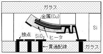
")
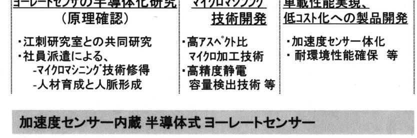
2 MEMS : MEMS ( +13% / ) 2
3 3

 p.741) (M.")

4 ISFET ph,co 2 (K.Shimada, M.Esashi, Med.& Biol.Eng.& Comp.,18 (1980) p.741) (M.Esashi T.Matsuo, Supplement to the J.J.AP.,44 (1975), ) 4
5 5

")
6 (Y.Matsumoto, S.Shoji, M.Esashi, 22nd Conference on Solid State Devices and Materials (1990) 701) 6
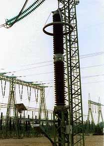
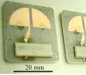
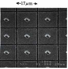
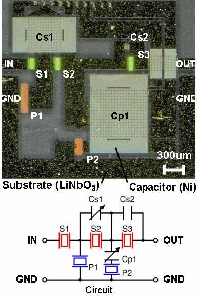
7 (1000V) (DC~10GHz) LSI MEMS (MEMS )( ) 7


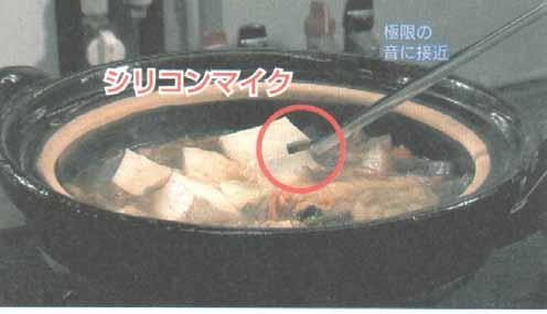
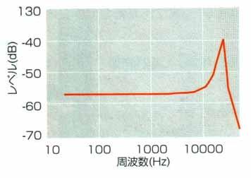
8 (NHK, ) (T.Tajima (NHK), M.Esashi et.al., Microelectronic Engineering, (2003) 508) 8
 (3MPa)")


 Thin Solid Films, 259")
9 SiO 2 LPCVD (650 ) 125nm Si poly-si (1000 ) (3MPa) ( m / min) Si (M.Kirsten, B.Wenk (Fraunhofer-Inst.), F.Ericson, J.A.Schweitz (Uppsala Univ.) Thin Solid Films, 259 (1995) pp ) ST Microelectronics 9
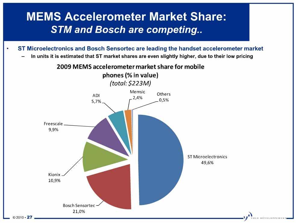
10 (J.C.Eloy, SEMICON Japan 2010)


11 (M.Nagao et.al.,sae World Congress, Detroit, (2004)) 11


12 2 (IDG-1000) ( ) (J.Seeger, M.Lim and S.Nasiri : Technical Digest Solid-State Sensor, Actuator and Microsystems Workshop, Hilton Head Island, 61 (2010) ) 12
 ( ) MESAG-100")


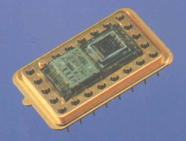
13 1.5mm 7.4 ( ) ( ) MESAG-100 (Micro Electrostatically Suspended Accelerometer Gyro) ( ) 13 (T.Murakoshi, Jpn. J. Appli. Phys., 42, Part1 No.4B (2003) p.2468)
14 ( ) 14
 ) 15")
15 (T.Katsumata et.al., Optical MEMS 97) (K. Totsu et.al., Transducers 03 (2003) ) 15
 (Magnetic Resonance")

16 / ~10 18 g 400 m 0.2 m f 0 =669.5Hz Q=1325 NdFeB (10 m ) (Magnetic Resonance Force detective Microscope (MRFM)) (T.Ono and M.Esashi, Rev. of Scientific Instruments, 74 (2003) 5141) 16
17 MRFM 17

 DPPH")
18 Optical image 10 m (MRFM) (ESR) DPPH (diphenylpicrylhydrazil))( ) 18
 (S.")

 p.")
19 (1 ) (NEC) (S.Tohyama, Optical Engineering, 45 (2006) p ) 19
20 ( NEC) 20
21 64 64 ( ) (T.Shimizu ( ), SEMI Technology Symposium (STS) 2010) 21
22 4 22 SAW (J.Kuypers, APCOT2006 p.293)


23 SAW (S.Hashimoto, Proceedings of the 24th Sensor Symposium, (2007), p.267) 23


24 SAW (A.Randles, 2008 IEEE International Ultrasonic Symposium (2008) p.1124) 24

) 3 ( 33 1")
25 (N.Asada et.al., IEEE Trans. on Magnetics 30 (1994)) 3 ( 33 1 (2009) 41) 25
 40")

 04DL19")

26 Concept PZT CVD pixels (SVGA) 40 cm (H.Matsuo, Y.Kawai and M.Esashi : Jap. J. Appl. Phys, 49 (2010) 04DL19 ) (E.Kawasaki, H.Yamada and H.Hamanaka : IDW 09 (2009) 1345 ) 26
27 ( ) 27
 1999")

")

28 ( ) 1999 Star Wars : Episode 1 (George Lucas ) DLP DMD (Digital Micromirror Device)( TI ) 28


29 TiAl 3 DMD TiAl 3 (DLP) DMD TiAl 3 - (J.Tregilgas, Advanced materials and Processes, (2005 Jan.) 45-49) 29
")
,")

30 FBAR (Film Balk Acoustic Resonator) LSI LSI (T.Matsumura (NICT), 2009 IEEE Internl. Ultrasonic Symp. (2009) 2141) 30
 (SAW) LSI")


31 LSI SAW (502 MHz) (SAW) LSI (K. D. Park, IEEJ The 26th Sensor Symposium, 37 (2009) 31

32 MEMS SAW (T.Yasue, Transducers 2011) 32
33 Au 33
 LTCC AuSn LTCC h 1 h 2 NPG Si (NPG) ENAS ) 34 (Y.-C. Lin, W.-S. Wang et.al.")
34 Au/Cr Through via hole NPG LTCC Au Photoresist LTCC LTCC h 2 h 2 > h 1 h 1 Si Au-Sn LTCC MEMS components Mechanical sealing frame Pressure, voltage and heat (Sn ) LTCC AuSn LTCC h 1 h 2 NPG Si (NPG) ENAS ) 34 (Y.-C. Lin, W.-S. Wang et.al., Transducers 2011)

35 6 / ( 1039, 2010/9/20) 35
 13,000 Y 2 m X 22nm (30nm")
 / Mapper ( http://www.")
36 Beam Blanker Array 1.4mm 1.5mm (110 ) 13,000 Y 2 m X 22nm (30nm LS ) (5kV) 0.3nA 10 (300mm ) / Mapper ( (EB) ( EB ( ) (2009) p.158) 36
, J. Vac. Sci. Technol.")
37 10 mm Si (A Kojima, H. Ohyi and N. Koshida ( ), J. Vac. Sci. Technol., 37 B26, 6 (2008) 2064)
38 ( ) 38
39 MEMS PC (80 ) MEMS (MEMSPC) MEMS (20mm ) (MNC) (2 LSI )) ( SIC) ( (4/6 )) (4/6 ) U.C.Berkeley MEMS MEMS Industry Group IMEC NICT LETI MEMS 39


40 2 ( ) (,,,, vol.10, no10, pp.32-35, Oct.1990.) 40
41 ( ) 41

42 ( ) 42
 ( )")
 MEMS")
")
43 (MNC) (2 LSI ) ( ) (4/6 MEMS ) MEMS MEMS MEMS (20mm ) (8 ) 43


44 ( ) 4 Tr 4/6 MEMS 44
45 ( ) 45
46 ( ) 46

47 IMEC ) IMEC Strategic Partner ( (EPFL)) 47
48 48

49 49
50 ) MEMS ( CD) ( ) / / / / / / MEMS (MEMSPC) MEMS 50


")
51 MEMS ican ican LED 2 ican ican ican2009 ican 11 (2010/9/3) ICAN MEMS 51

52
53 53

54 ( ) ( )
untitled
 1. 2. ( ) 3. ( ) 4. ( ) 5. ( ) 6. MEMS 20mm 400 (40 )100 A-A A 2. ( ) MEMS A (L.M.Roylance et.al., IEEE Trans. on Electron Devices, ED-26 (1979) p.1911) ( (In-Vivo Oximetry)) (J.M.Schmitt,F.G.Mihm and
( )
") MEMS 4 : ( ) ( ) Pt ITO Si (2 m) Si (0.2 m) (T.Ono et.al., J.Micromech.Microeng.,10 (2000) 445-451) DEMA (Distributed Electrostatic MicroActuator) (XY ) DEMA (Distributed Electrostatic MicroActuator)
MEMS 4 : ( ) ( ) Pt ITO Si (2 m) Si (0.2 m) (T.Ono et.al., J.Micromech.Microeng.,10 (2000) 445-451) DEMA (Distributed Electrostatic MicroActuator) (XY ) DEMA (Distributed Electrostatic MicroActuator)
) ( ) ( 34,3 (1995))
 ( ) ( 34,3 (1995))") 4. MEMS 2 : MEMS ( ) DMD (Digital Micro mirror Device) FED (Field Emission Display) ( ) ( ) RF ( ) ( ) IC RF ( ) ) ( ) ( 34,3 (1995)) (M.Murata et.al.: IEICE Trans. Electron., E84-c (2001) p.1792) ( )
4. MEMS 2 : MEMS ( ) DMD (Digital Micro mirror Device) FED (Field Emission Display) ( ) ( ) RF ( ) ( ) IC RF ( ) ) ( ) ( 34,3 (1995)) (M.Murata et.al.: IEICE Trans. Electron., E84-c (2001) p.1792) ( )
IC NMOS ( )
") 5. MEMS 3 : IC NMOS ( ) (T.Hoshino (Tokyo Electron Ltd.) et.al., 18 th Sensor Symposium late news, 2001) 10000 memory : Probe (pad) Count 4000 Cobra probe cards 2000 ASIC 200 LCD driver IC Epoxy-needle
5. MEMS 3 : IC NMOS ( ) (T.Hoshino (Tokyo Electron Ltd.) et.al., 18 th Sensor Symposium late news, 2001) 10000 memory : Probe (pad) Count 4000 Cobra probe cards 2000 ASIC 200 LCD driver IC Epoxy-needle
) ( ) ( 34,3 (1995))
 ( ) ( 34,3 (1995))") 4. MEMS 2 : MEMS ( ) DMD (Digital Micro mirror Device) FED (Field Emission Display) ( ) ( ) RF ( ) ( ) IC RF ( ) ) ( ) ( 34,3 (1995)) (M.Murata et.al.: IEICE Trans. Electron., E84-c (2001) p.1792) ( )
4. MEMS 2 : MEMS ( ) DMD (Digital Micro mirror Device) FED (Field Emission Display) ( ) ( ) RF ( ) ( ) IC RF ( ) ) ( ) ( 34,3 (1995)) (M.Murata et.al.: IEICE Trans. Electron., E84-c (2001) p.1792) ( )
c c SSIS10 10 10 1998 2001 SSIS 2001 LSI 2001 MIRAI NECASKA SELETE 21 5ISSCC LSI 2004 2004SSIS PR 60 70
 Encore SSIS 10 c c SSIS10 10 10 1998 2001 SSIS 2001 LSI 2001 MIRAI NECASKA SELETE 21 5ISSCC LSI 2004 2004SSIS PR 60 70 SSIS NOSIDE PR SSIS SSIS PR 2000 5SSIS SSIS 1 2001 5 8 3 2004 SSIS 1 2 SSIS 24 SSISPR

2 ( ) PVD (Physical Vapor Deposition)
 PVD (Physical Vapor Deposition)") 2 ( ) PVD (Physical Vapor Deposition) G.Lim et.al., Robotica, 14 (1996) pp.499-506 ( ) ( Ionics, 20, 9 (1994) p.147) MEMS CVD (Chemical Vapor Deposition) CVD MacDonald et.al. MEMS 90 CVD 160-220ºC 1,1,1,5,5,5,5-
2 ( ) PVD (Physical Vapor Deposition) G.Lim et.al., Robotica, 14 (1996) pp.499-506 ( ) ( Ionics, 20, 9 (1994) p.147) MEMS CVD (Chemical Vapor Deposition) CVD MacDonald et.al. MEMS 90 CVD 160-220ºC 1,1,1,5,5,5,5-
IC NMOS ( )
") 5. MEMS 3 : IC NMOS ( ) (T.Hoshino (Tokyo Electron Ltd.) et.al., 18 th Sensor Symposium late news, 2001) 10000 memory : Probe (pad) Count 4000 Cobra probe cards 2000 ASIC 200 LCD driver IC Epoxy-needle
5. MEMS 3 : IC NMOS ( ) (T.Hoshino (Tokyo Electron Ltd.) et.al., 18 th Sensor Symposium late news, 2001) 10000 memory : Probe (pad) Count 4000 Cobra probe cards 2000 ASIC 200 LCD driver IC Epoxy-needle
sumi.indd
 S/N S/N CCDCMOS CCD CMOS & E-mail hirofumi.sumi@jp.sony.com & E-mail Tadakuni.Narabu@jp.sony.com & E-mail Shinichiro.Saito@jp.sony.com Hirofumi SUMI, Non - Member and Tadakuni NARABU, Member and Shinichiro
スライド 1
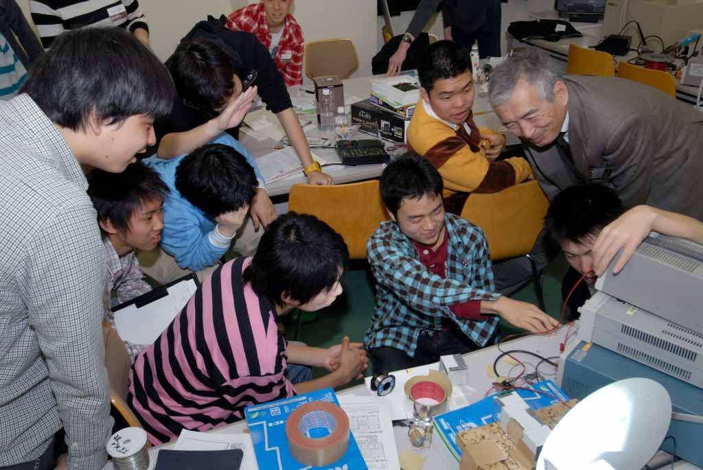
 ( 第 16 回 ) MEMS 集中講義 in 豊田工大プログラム 8 月 2 日 ( 木 ) 10:00-10:30 1. MEMS マイクロマシニングの概論 [ 江刺 ] 10:30-12:00 2. 豊田工大と その施設および MEMS 研究の紹介 [ 豊田工大佐々木 ] 12:00-13:30 昼食 (30 分 ) 研究室見学 (15 分 ) CR 見学 (25 分 )(3 グループ分割で順序入替により混雑回避
i
 i ii 1 6 9 12 15 16 19 19 19 21 21 22 22 23 26 32 34 35 36 3 37 5 5 4 4 5 iii 4 55 55 59 59 7 7 8 8 9 9 10 10 1 11 iv ozein Van Marum 1801 Cruiokshank Marum 1840 Schonbein 3 / atm 1 N 1892 50 1960 1970
 1-x x µ (+) +z µ ( ) Co 2p 3d µ = µ (+) µ ( ) W. Grange et al., PRB 58, 6298 (1998). 1.0 0.5 0.0 2 1 XMCD 0-1 -2-3x10⁻³ 7.1 7.2 7.7 7.8 8.3 8.4 up E down ρ + (E) ρ (E) H, M µ f + f E F f + f f + f X L
16 (16) poly-si mJ/cm 2 ELA poly-si super cooled liquid, SCL [3] a-si poly-si [4] solid phase crystalization, SPC [5] mJ/cm 2 SPC SCL (di
![16 (16) poly-si mJ/cm 2 ELA poly-si super cooled liquid, SCL [3] a-si poly-si [4] solid phase crystalization, SPC [5] mJ/cm 2 SPC SCL (di](/thumbs/82/84964999.jpg "16 (16) poly-si mJ/cm 2 ELA poly-si super cooled liquid, SCL [3] a-si poly-si [4] solid phase crystalization, SPC [5] mJ/cm 2 SPC SCL (di") (15) 15 ELA により形成された poly-si 結晶成長様式 - グレイン形状と水素の関係 - Crystal Growth Mode of Poly-Si Prepared by ELA -Relationship between the Grain Morphology and ydrogens- Naoya KAWAMOTO (Dept. of Electrical and Electronic
(15) 15 ELA により形成された poly-si 結晶成長様式 - グレイン形状と水素の関係 - Crystal Growth Mode of Poly-Si Prepared by ELA -Relationship between the Grain Morphology and ydrogens- Naoya KAWAMOTO (Dept. of Electrical and Electronic
研究成果報告書
 10m 2m Ge Si BaF2 ZnSZnSe Sb-Ge-Sn-S IIR-SF1 1 2 Tungsten SilicideWSi WSi () IIR-SF 1 Sb-Ge-Sn-S 0.85~11μm2.710μm 253 C Al Al 220μm He-Cd laser 1 Exposure Photoresist WSi (a) 500 nm Development RIE WSi
1).1-5) - 9 -
.1-5) - 9 -") - 8 - 1).1-5) - 9 - ε = ε xx 0 0 0 ε xx 0 0 0 ε xx (.1 ) z z 1 z ε = ε xx ε x y 0 - ε x y ε xx 0 0 0 ε zz (. ) 3 xy ) ε xx, ε zz» ε x y (.3 ) ε ij = ε ij ^ (.4 ) 6) xx, xy ε xx = ε xx + i ε xx ε xy = ε
- 8 - 1).1-5) - 9 - ε = ε xx 0 0 0 ε xx 0 0 0 ε xx (.1 ) z z 1 z ε = ε xx ε x y 0 - ε x y ε xx 0 0 0 ε zz (. ) 3 xy ) ε xx, ε zz» ε x y (.3 ) ε ij = ε ij ^ (.4 ) 6) xx, xy ε xx = ε xx + i ε xx ε xy = ε
技術調査レポート(セット版)0318
0318") 1 MEMS MEMS(Micro Electro Mechanical Systems) MEMS MEMS 1990 MEMS MEMS 2 MEMS MEMS MEMS mm ( ) MEMS MST 1mm 1m Ball Semiconductor Inc. IC [2] IC [2] Si 3 MEMS 2.1 MEMS DNA MEMS 80 MEMS ABS 2.0mm 15mm 4
1 MEMS MEMS(Micro Electro Mechanical Systems) MEMS MEMS 1990 MEMS MEMS 2 MEMS MEMS MEMS mm ( ) MEMS MST 1mm 1m Ball Semiconductor Inc. IC [2] IC [2] Si 3 MEMS 2.1 MEMS DNA MEMS 80 MEMS ABS 2.0mm 15mm 4
日立評論2008年1月号 : 基盤技術製品
 Infrastructure Technology / Products HIGHLIGHTS 2008 HDD 2.5 HDD3.5 HDD 1 Deskstar 7K1000 HDD Hard Disk Drive 2006 5 PC 2.5 HDD HDD 3.5 HDD1 1 2007 3Deskstar 7K1000 3.5 HDD 1149 Deskstar 7K500 2 GMR Giant
スライド 1
 swk(at)ic.is.tohoku.ac.jp 2 Outline 3 ? 4 S/N CCD 5 Q Q V 6 CMOS 1 7 1 2 N 1 2 N 8 CCD: CMOS: 9 : / 10 A-D A D C A D C A D C A D C A D C A D C ADC 11 A-D ADC ADC ADC ADC ADC ADC ADC ADC ADC A-D 12 ADC
10 nm SThM Fig.1 AFM 6) AFM 7) Fig.1 AFM 0.1 N/m 100 pn 10 nn 8) SThM STM AFM RTD Resistance Temperature Device SNOM Scanning Near-field Optical Micro
 AFM 7) Fig.1 AFM 0.1 N/m 100 pn 10 nn 8) SThM STM AFM RTD Resistance Temperature Device SNOM Scanning Near-field Optical Micro") @@@@@@@@@@@@@@ @@@@@@@@@@@@@@@@@@@@@@@@@@@@@@@@@@@@@@@@@@@@@@@@@@@@@@@@@@@@@@@@@@@@@@@@@@@@@@@@@@@@@@@@@@@@@@@@@@@@@@@@@@@@@@@@@@@@@@@@@@@@@@@@@@@@@@@@@@@@@@@@@@@@@@@@@@@@@@@@@@@@@@@@@@@@@@@@@@@@@@@@@@@@@@@@@@@@@@@@@@@@@@@@
@@@@@@@@@@@@@@ @@@@@@@@@@@@@@@@@@@@@@@@@@@@@@@@@@@@@@@@@@@@@@@@@@@@@@@@@@@@@@@@@@@@@@@@@@@@@@@@@@@@@@@@@@@@@@@@@@@@@@@@@@@@@@@@@@@@@@@@@@@@@@@@@@@@@@@@@@@@@@@@@@@@@@@@@@@@@@@@@@@@@@@@@@@@@@@@@@@@@@@@@@@@@@@@@@@@@@@@@@@@@@@@
 Jan. 2005 Jan. 2005 2 4 12 13 23 29 42 47 52 58 59 68 95 96 69 72 77 78 83 84 2 / 3 4 Vol.78 No.1 2005 5 6 Vol.78 No.1 2005 A040728 0043 7 V 8 Vol.78 No.1 2005 9 µ 10 Vol.78 No.1 2005 µ 11 12 Vol.78 No.1
2). 3) 4) 1.2 NICTNICT DCRA Dihedral Corner Reflector micro-arraysdcra DCRA DCRA DCRA 3D DCRA PC USB PC PC ON / OFF Velleman K8055 K8055 K8055
. 3) 4) 1.2 NICTNICT DCRA Dihedral Corner Reflector micro-arraysdcra DCRA DCRA DCRA 3D DCRA PC USB PC PC ON / OFF Velleman K8055 K8055 K8055") 1 1 1 2 DCRA 1. 1.1 1) 1 Tactile Interface with Air Jets for Floating Images Aya Higuchi, 1 Nomin, 1 Sandor Markon 1 and Satoshi Maekawa 2 The new optical device DCRA can display floating images in free
1 1 1 2 DCRA 1. 1.1 1) 1 Tactile Interface with Air Jets for Floating Images Aya Higuchi, 1 Nomin, 1 Sandor Markon 1 and Satoshi Maekawa 2 The new optical device DCRA can display floating images in free


土木工事共通仕様書(その2)
") 2 3 4 5 6 7 8 9 10 11 12 13 14 15 16 17 18 19 1 2 3 22 578 582 27 4 5 6 567 7 21 8 9 (9), 10 11 12 13 14 (1) (2) 16 532 35 15 (3) (4) (1) (1) 16 (4) () () () 17 () 18 170 19 20 21 10 22 23 24 25 26 27
2 3 4 5 6 7 8 9 10 11 12 13 14 15 16 17 18 19 1 2 3 22 578 582 27 4 5 6 567 7 21 8 9 (9), 10 11 12 13 14 (1) (2) 16 532 35 15 (3) (4) (1) (1) 16 (4) () () () 17 () 18 170 19 20 21 10 22 23 24 25 26 27

The Plasma Boundary of Magnetic Fusion Devices
 ASAKURA Nobuyuki, Japan Atomic Energy Research Institute, Naka, Ibaraki 311-0193, Japan e-mail: asakuran@fusion.naka.jaeri.go.jp The Plasma Boundary of Magnetic Fusion Devices Naka Fusion Research Establishment,


& Vol.5 No (Oct. 2015) TV 1,2,a) , Augmented TV TV AR Augmented Reality 3DCG TV Estimation of TV Screen Position and Ro
 TV 1,2,a) , Augmented TV TV AR Augmented Reality 3DCG TV Estimation of TV Screen Position and Ro") TV 1,2,a) 1 2 2015 1 26, 2015 5 21 Augmented TV TV AR Augmented Reality 3DCG TV Estimation of TV Screen Position and Rotation Using Mobile Device Hiroyuki Kawakita 1,2,a) Toshio Nakagawa 1 Makoto Sato
TV 1,2,a) 1 2 2015 1 26, 2015 5 21 Augmented TV TV AR Augmented Reality 3DCG TV Estimation of TV Screen Position and Rotation Using Mobile Device Hiroyuki Kawakita 1,2,a) Toshio Nakagawa 1 Makoto Sato

untitled
 TOKUSHIMA PREFECTURAL INDUSTRIAL TECHNOLOGY CENTER 1 1 1 2 3 4 2 6 7 2 9 7 1 8 9 9 7 1 8 5 1 6 4 4 5 42 7 5 3 10 7 4 3 32 15 73 40 208 236 55 120 747 96 233 1,107 1,133 1,282 712 875 5,438 11 1,889 817
 (2) (3) (4) (5) 2.1 ( ) 2")
 10 117 5 1 121841 4 15 12 7 27 12 6 31856 8 21 1983-2 - 321899 12 21656 2 45 9 2 131816 4 91812 11 20 1887 461971 11 3 2 161703 11 13 98 3 16201700-3 - 2 35 6 7 8 9 12 13 12 481973 12 2 571982 161703 11
0.45m1.00m 1.00m 1.00m 0.33m 0.33m 0.33m 0.45m 1.00m 2
 24 11 10 24 12 10 30 1 0.45m1.00m 1.00m 1.00m 0.33m 0.33m 0.33m 0.45m 1.00m 2 23% 29% 71% 67% 6% 4% n=1525 n=1137 6% +6% -4% -2% 21% 30% 5% 35% 6% 6% 11% 40% 37% 36 172 166 371 213 226 177 54 382 704 216
10 IDM NEC
 No.29 1 29 SEAJ SEAJ 2 3 63 1 1 2 2002 2003 6 News 9 IEDM 11 13 15 16 17 10 IDM NEC 3 12 3 10 10 2 3 3 20 110 1985 1995 1988 912001 1 1993 95 9798 199010 90 200 2 1950 2 1950 3 1311 10 3 4 4 5 51929 3
(a) 1 (b) 3. Gilbert Pernicka[2] Treibitz Schechner[3] Narasimhan [4] Kim [5] Nayar [6] [7][8][9] 2. X X X [10] [11] L L t L s L = L t + L s
![(a) 1 (b) 3. Gilbert Pernicka[2] Treibitz Schechner[3] Narasimhan [4] Kim [5] Nayar [6] [7][8][9] 2. X X X [10] [11] L L t L s L = L t + L s](/thumbs/75/72066128.jpg "(a) 1 (b) 3. Gilbert Pernicka[2] Treibitz Schechner[3] Narasimhan [4] Kim [5] Nayar [6] [7][8][9] 2. X X X [10] [11] L L t L s L = L t + L s") 1 1 1, Extraction of Transmitted Light using Parallel High-frequency Illumination Kenichiro Tanaka 1 Yasuhiro Mukaigawa 1 Yasushi Yagi 1 Abstract: We propose a new sharpening method of transmitted scene
1 1 1, Extraction of Transmitted Light using Parallel High-frequency Illumination Kenichiro Tanaka 1 Yasuhiro Mukaigawa 1 Yasushi Yagi 1 Abstract: We propose a new sharpening method of transmitted scene
Introduction to Microfabrication
 2005 Introduction to Microfabrication 1 1.1 Microfabrication disciplines Microfabrication technologies IC industry and related industries MEMS, solar cells, flat-panel displays, optelectronics In-plane
技術創造の社会的条件
 1999 10 21 21 i ... 1 1... 3 1-1. 20...3 1900 1945 3 1945 198x 4 198x 1999 5 1-2....7 1945 198x 7 HEMT 8 198x 1999 9 9 1-3....11 11 12 13 18 2 New Institutions... 21 2-1....21 22 24 26 2-2....27 28 29
Microsoft PowerPoint - presen_dist.ppt
 LSI 技術とセンサー技術の融合による インテリジェントスマートマイクロチップ 豊橋技術科学大学 赤井大輔 澤田和明 akai@vbl.tut.ac.jp http://www.vbl.tut.ac.jp/ 高性能 独創的なデバイスの実現 - イメージセンサの例 - CCD 型 高性能 特殊プロセス CMOS 型 低性能, 安価 CMOS 周辺回路との融合 高性能化のために プロセスの特殊化 材料の特殊化
支援財団研究活動助成 生体超分子を利用利用した 3 次元メモリデバイスメモリデバイスの研究 奈良先端科学技術大学院大学物質創成科学研究科小原孝介
 2009.3.10 支援財団研究活動助成 生体超分子を利用利用した 3 次元メモリデバイスメモリデバイスの研究 奈良先端科学技術大学院大学物質創成科学研究科小原孝介 研究背景研究背景研究背景研究背景データデータデータデータの種類種類種類種類データデータデータデータの保存保存保存保存パソコンパソコンパソコンパソコンパソコンパソコンパソコンパソコンデータデータデータデータデータデータデータデータ音楽音楽音楽音楽音楽音楽音楽音楽写真写真写真写真記録媒体記録媒体記録媒体記録媒体フラッシュメモリフラッシュメモリフラッシュメモリフラッシュメモリ動画動画動画動画
 1 1 2 3 4 5 6 7 8 9 10 11 12 13 14 15. 1. 2. 3. 16 17 18 ( ) ( 19 ( ) CG PC 20 ) I want some rice. I want some lice. 21 22 23 24 2001 9 18 3 2000 4 21 3,. 13,. Science/Technology, Design, Experiments,
untitled
 254nm UV TiO 2 20nm :Sr 5 Ta 4 O 15 3 4 KEY-1 KEY-2 (Ti,Nb,Ta) 5 KEY-1 KEY-2 6 7 NiO/ Sr 2 Ta 2 O 7 mmol h -1 g -1 20 15 10 5 H 2 O 2 H 2 O 2 0 0 2 4 6 8 10 12 NiO/Sr 2 Ta 2 O 7 The synthesis of photocatalysts
** Department of Materials Science and Engineering, University of California, Los Angeles, CA 90025, USA) Preparation of Magnetopulmbite Type Ferrite
 Preparation of Magnetopulmbite Type Ferrite") ** Department of Materials Science and Engineering, University of California, Los Angeles, CA 90025, USA) Preparation of Magnetopulmbite Type Ferrite Thin Films by Dip-Coating Method and Magnetic Properties
** Department of Materials Science and Engineering, University of California, Los Angeles, CA 90025, USA) Preparation of Magnetopulmbite Type Ferrite Thin Films by Dip-Coating Method and Magnetic Properties
untitled
 2013 74 Tokyo Institute of Technology AlGaN/GaN C Annealing me Dependent Contact Resistance of C Electrodes on AlGaN/GaN, Tokyo Tech.FRC, Tokyo Tech. IGSSE, Toshiba, Y. Matsukawa, M. Okamoto, K. Kakushima,
Siマイクロマシニングと集積化技術.PDF
 ケミカル エンジニアリング(化学工業社) 25 年 9 月号 pp.731-735. シリコンマイクロマシニングと集積化技術 佐々木実*1 金森義明*2 羽根一博*3 Minoru Sasaki, Yoshiaki Kanamori, Kazuhiro Hane 東北大学大学院工学研究科 *1 助教授 工学博士 *2 助手 工学博士 *3 教授 工学博士 1 はじめに LSI に代表される半導体産業の黎明期にフォト
第122号.indd
 -1- -2- -3- 0852-36-5150 0852-36-5163-4- -5- -6- -7- 1st 1-1 1-2 1-3 1-4 1-5 -8- 2nd M2 E2 D2 J2 C2-9- 3rd M3 E3 D3 J3 C3-10- 4th M4 E4 D4 J4 C4-11- -12- M5 E5 J5 D5 C5 5th -13- -14- NEWS NEWS -15- NEWS
研究成果報告書(基金分)
") (DMS) 1 3 DMS 2 4 DMS II-VI CdTe ZnTe 2 4 DMS 2 4 DMS II-VI 2 3d 4 3d (MBE) II-VI ZnTe CdTe 3d Mn, Cr, Fe 2 4 DMS MBE X (XRD)X (XAFS) II (SQUID) (a) 4 DMS (Cd,Mn,Cr)Te 4 DMS II-VI CdTe 2 Mn, Cr (Cd,Mn,Cr)Te
(DMS) 1 3 DMS 2 4 DMS II-VI CdTe ZnTe 2 4 DMS 2 4 DMS II-VI 2 3d 4 3d (MBE) II-VI ZnTe CdTe 3d Mn, Cr, Fe 2 4 DMS MBE X (XRD)X (XAFS) II (SQUID) (a) 4 DMS (Cd,Mn,Cr)Te 4 DMS II-VI CdTe 2 Mn, Cr (Cd,Mn,Cr)Te
 J60335-1(3 ) 250 480 IEC 60065 IEC 60601 IEC 60745 IEC 60950 IEC 61029 2.1 2.2.1 2.2.2 2.2.3 2.2.4 2.2.5 2.2.6-1- J60335-1(3 ) 2.2.7 2.2.8 2.2.9 2.3.1 2.3.2 2.3.3 2.3.4 2.3.5 2.3.6 2.3.7 2.4.1 2.4.2 2.4.3
IPSJ SIG Technical Report Vol.2014-DPS-158 No.27 Vol.2014-CSEC-64 No /3/6 1,a) 2,b) 3,c) 1,d) 3 Cappelli Bazen Cappelli Bazen Cappelli 1.,,.,.,
 2,b) 3,c) 1,d) 3 Cappelli Bazen Cappelli Bazen Cappelli 1.,,.,.,") 1,a),b) 3,c) 1,d) 3 Cappelli Bazen Cappelli Bazen Cappelli 1.,,,,,.,,,,.,,.,,,,.,, 1 Department of Electrical Electronic and Communication Engineering Faculty of Science and Engineering Chuo University
1,a),b) 3,c) 1,d) 3 Cappelli Bazen Cappelli Bazen Cappelli 1.,,,,,.,,,,.,,.,,,,.,, 1 Department of Electrical Electronic and Communication Engineering Faculty of Science and Engineering Chuo University
2002~2004年ハンセン病関係資料撮影リスト
 3 13 2 2002 2004 14510356 2002 2004 1 15 2003 5 1 3,758 70 51.27 1 2003 1 31 http://www.mhlw.go.jp 2005 3 1 http://www.jlf.or.jp/work/hansen_report.shtml 1981 50 1982 1982 1993 1993 1991 1982 ) 1 2 2002
42 1 Fig. 2. Li 2 B 4 O 7 crystals with 3inches and 4inches in diameter. Fig. 4. Transmission curve of Li 2 B 4 O 7 crystal. Fig. 5. Refractive index
 MEMOIRS OF SHONAN INSTITUTE OF TECHNOLOGY Vol. 42, No. 1, 2008 Li 2 B 4 O 7 (LBO) *, ** * ** ** Optical Scatterer and Crystal Growth Technology of LBO Single Crystal For Development with Optical Application
untitled
 1 1-1 p-i-n 1-1 (CIS/CIGS CdTe ) (GaAs) (,,) (, ) (,,) Si Si Si (CIS/CIGS CdTe ) (GaAs) (,,) (, ) (,,) Si Si Si Si 1-2 HITHeterojunction with Intrinsic Thin layer 30 HIT 22.3NIKKEI MICRODEVICES, May,82-86(2008)
理工ジャーナル21‐2/付録(21‐2)
") 2008 2009 3 31 B 1 10 B 1 10 B 1 10 B 1 10 B 1 10 10 B 1 NEC 10 B 1 10 B 1 10 B 1 10 B 1 10 10 B 1 10 B 1 10 B 1 10 B 1 11 B 1 10 C 1 10 C 1 11 C 1 11 C 21 10 C 21 10 C 21 10 C 21 10 C 21 10 C 21 11 C
2008 2009 3 31 B 1 10 B 1 10 B 1 10 B 1 10 B 1 10 10 B 1 NEC 10 B 1 10 B 1 10 B 1 10 B 1 10 10 B 1 10 B 1 10 B 1 10 B 1 11 B 1 10 C 1 10 C 1 11 C 1 11 C 21 10 C 21 10 C 21 10 C 21 10 C 21 10 C 21 11 C
第1章 溶接法および機器
 670 ) ) ) ) 2.1 ) 42 671 Sn T m K. T m. T m. T m 2.2 JIS BAl BPd Al-Si Al-Mn KAlF -K AlF H O Ni 43 672 Sn-In Zn EU RoHS ) Pb Cd Hg JIS Z ( ) ) ) 3.1 44 673. MO HX MX H O M X (d) Young sf lf cos sl sf lf
13 EUVA EUV EUVLL (NEDO) EUV (EUVA) 10 EUVA EUV W EUV EUV LPP EUV DPP EUVA 2 Selete 26nm IMEC EUVA NEDO
 EUV (EUVA) 10 EUVA EUV W EUV EUV LPP EUV DPP EUVA 2 Selete 26nm IMEC EUVA NEDO") 13 EUVA EUV EUVLL 2002 6 (NEDO) EUV (EUVA) 10 EUVA 2002 2005 EUV 2007 2 2005 1050W EUV EUV LPP EUV DPP EUVA 2 Selete 26nm IMEC 1 2008 2010 EUVA NEDO EUVA EUV 2006 Selete EUVA 1. EUVA 436nm 365nm 1/17 KrF
13 EUVA EUV EUVLL 2002 6 (NEDO) EUV (EUVA) 10 EUVA 2002 2005 EUV 2007 2 2005 1050W EUV EUV LPP EUV DPP EUVA 2 Selete 26nm IMEC 1 2008 2010 EUVA NEDO EUVA EUV 2006 Selete EUVA 1. EUVA 436nm 365nm 1/17 KrF

HDD 1-1 HDD HDD 1-2 1-1 HDD () 25-515578 1-2 1
 25-515578 1-2 1") HDD 1-1 HDD HDD 1-2 1-1 HDD () 25-515578 1-2 1 1-3 HDD 1-3 HDD GMR 1-4 HDD HD-DVD Blu-ray Disc HDD 25 HDD 26 TMR 1975 3 25 26 Seagate Technology ( GST) 3 HDD HDD 1-4 HDD 13Gb/inch 2 3 HDD TMR 2 HDD HDD
HDD 1-1 HDD HDD 1-2 1-1 HDD () 25-515578 1-2 1 1-3 HDD 1-3 HDD GMR 1-4 HDD HD-DVD Blu-ray Disc HDD 25 HDD 26 TMR 1975 3 25 26 Seagate Technology ( GST) 3 HDD HDD 1-4 HDD 13Gb/inch 2 3 HDD TMR 2 HDD HDD
PowerPoint プレゼンテーション
 2004 SPring-8 2004/6/21 CMOS 2004 2007 2010 2013 nm 90 65 45 32 (nm) 1.2 0.9 0.7 0.6 High-performance Logic Technology Requirements (ITRS 2003) 10 Photoelectron Intensity (arb.units) CTR a-sio2 0.1 HfO
07.報文_及川ら-二校目.indd
 8 01 01 4 4 1 5 16 18 6 006 H 18 4 011 H 6 4 1 5 1 5 007 H 19 5 009 1 5 006 007 009 011 9 10 4 000 H 1 4 5 004 H 16 4 004 009 H 1 5 4 4 5 1 4 006 011 1 1 4m 5m 10m 007 1 7 009 009 1 5 10 1 000kg 10a 006
ST 1 MOS MOS 1 1 2 8 1 CMOS CMOS 7mm3mm LSI 10 SSIS
 No.28 1 SSIS 5 244 38 1600 SSIS 53 2 SSIS Human Net Work Knowledge Chain 3 11 1 SSIS OB SSIS 1 NoSide 2 5 2003 7 RCA 9 11 12 13 ST 1 MOS MOS 1 1 2 8 1 CMOS CMOS 7mm3mm LSI 10 SSIS 21 GM RCA IBM GE WE 20
untitled
 2009 7 29-30 1 2 + + = 1 = 1 ( = = 0) 3 Eb (, T ) exp[ C C 2 1 5 /( T )] 1 [ W/(m2μm)] : [ m] T : [K] C 1 = 3.743 10 8 [W m 4 /m 2 ] C 2 = 1.439 10 4 [ m K] 4 E b max max T 2897 m m K = 10 m 5 E E b E
2章.doc
 C 2 H 4 N 2 O 2 LPG LIF 13 2.1 2.1.1 2.1 2.2 115mm70mm 727cm 3 Hand Pump Injector Driver Computer Constant Volume Chamber Injector Piezo-electronic transducer Fan Spark Plug Temperature Indicator C 2 H
untitled
 2006.2.27 Fantastic Voyage 1966 1 2006.2.27 Fantastic Voyage 2006.2.27 2 2006.2.27 How Small is Micro & Nano? 1mm 10µm 2nm 1m DNA 10 2 10 10 0 10-1 10-2 10-3 10-4 10-5 10-6 10-7 10-8 10-9 10-10 (m) Macroscopic
Fundamental Study on the SOX Gas Sensor Utilizing Beta-Alumina with Sputtered Praseodymium Oxide Thin Films by Shinya YAO1*, Kenji MIYAGAWA1, Shigeru
 Fundamental Study on the SOX Gas Sensor Utilizing Beta-Alumina with Sputtered Praseodymium Oxide Thin Films by Shinya YAO1*, Kenji MIYAGAWA1, Shigeru IIJIMA2 and Zensaku KOZUKA1 1. Faculty of Engineering,
JAJP
 Agilent 7500ce ORS ICP-MS Glenn Woods Agilent Technologies Ltd. 5500 Lakeside, Cheadle Royal Business Park Stockport UK Agilent 7500ce ICP-MS 5 7500ce (ORS) 1 ORS 7500ce ORS ICP-MS ( ) 7500 ICP-MS (27.12
20 m Au 2. 現行のマイクロバンプ形成技術における課題 Au Au Au 2 WB 11 m m 1 m 2008 Au FC m 10 m 30 m OTK Au 表 1 マイクロバンプ形成におけるめっき法の比較 3. 無電解めっきによる Au
 Fabrication technology of Au micro-bump by electroless plating. 関東化学株式会社技術 開発本部中央研究所第四研究室德久智明 Tomoaki Tokuhisa Central Research Laboratory, Technology & Development Division, Kanto Chemical Co., Inc. 1.
理工ジャーナル 24‐2☆/大トビラ
 2011 00009 10 00009 10 00010 20 00010 20 00010 10 00010 10 00010 10 00010 10 00010 NEC 10 00010 NTT 10 00011 11 00011 11 00011 10 00011 10 00012 10 00013 10 00017 10 00018 11 00021 10 00021 11 00023 11
The Recording Industry in Japan Statistics Analysis Trends 2005
 The Recording Industry in Japan Statistics Analysis Trends 8cmCD cmcd cmcd CD DVD LD DVD LD,99,76,6 6,,6 66,47 78,9,9 8,8 4, 7,7,4 4,6 78,9, 6 9 894 8,98 9 8,999 7 6 4, 78,67,68 7, 6,,7, 8,8 6,9 4,77,68
 The Present Situation of Surface Treatment Technology for Stainless Steels Keinosuke TSUJI and Youichi NAKAGAWA Steel Co., Ltd., Now Osaka Branch) ( 1) Na2O 11.6, K2O 5.0, Al2O3 5.4, B2O3 8.6, SiO2 54.2,
 14 2 5 20 21 DNA 1 1 2 () () 3 4 5 4 J.R.Webster, M.A.Burms, D.T.Burke and C.H.Mastrangelo Center for Integrated Microsystems, Department of Electrical Engineering and Computer Science, Department of
 TOKUSHIMA PREFECTURAL INDUSTRIAL TECHNOLOGY CENTER 1 1 1 2 3 3 3 6 1 4 1 6 9 1 10 9 1 10 8 1 9 5 1 6 5 5 5 43 8 1 6 10 8 9 9 43 14 21 112 126 69 74 416 192 976 892 1,312 1,323 842 5,537 2,255 310 749
, [g/cm 3 ] [m/s] 1 6 [kg m 2 s 1 ] ,58 1, ,56 1, , ,58 1,
![, [g/cm 3 ] [m/s] 1 6 [kg m 2 s 1 ] ,58 1, ,56 1, , ,58 1,](/thumbs/70/63326930.jpg ", [g/cm 3 ] [m/s] 1 6 [kg m 2 s 1 ] ,58 1, ,56 1, , ,58 1,") 264 72 5 216 pp. 264 272 * 43.3. k, Yj; 43.38.Hz 1. 2. 2.1 1 4.8 1 2 [kg m 2 s 1 ] 1.2 1 3 [g/cm 3 ] 34 [m/s] 1.48 1 6 [kg m 2 s 1 ] 1 [g/cm 3 ] 1,48 [m/s] 1, 1 4 1 2,5 1 Tutorial on the underwater or
264 72 5 216 pp. 264 272 * 43.3. k, Yj; 43.38.Hz 1. 2. 2.1 1 4.8 1 2 [kg m 2 s 1 ] 1.2 1 3 [g/cm 3 ] 34 [m/s] 1.48 1 6 [kg m 2 s 1 ] 1 [g/cm 3 ] 1,48 [m/s] 1, 1 4 1 2,5 1 Tutorial on the underwater or
untitled
 /Si FET /Si FET Improvement of tunnel FET performance using narrow bandgap semiconductor silicide Improvement /Si hetero-structure of tunnel FET performance source electrode using narrow bandgap semiconductor
J. Jpn. Inst. Light Met. 65(6): 224-228 (2015)
: 224-228 (2015)") 65 62015 224 228 ** Journal of The Japan Institute of Light Metals, Vol. 65, No. 6 (2015), 224 228 2015 The Japan Institute of Light Metals Investigation of heat flow behavior on die-casting core pin with
65 62015 224 228 ** Journal of The Japan Institute of Light Metals, Vol. 65, No. 6 (2015), 224 228 2015 The Japan Institute of Light Metals Investigation of heat flow behavior on die-casting core pin with
 155 13 2 15 B97176 1 1.1. 4 1.2. 5 1.2.1. 1.2.2. 1.3. 7 2. 2.1. 9 2.2. 1 2.3. 13 2.4. 16 3. 3.1. 3.1.1. 18 3.1.2. 26 3.1.3. 33 3.2. 3.2.1. 34 3.2.2. 5 4. 4.1. 52 4.2. 53 54 55 2 1 1.1 1.2 1.3 3 4 Fig.
UL STYLE 1015LF, CSA TYPE TEW XLPE UL, CSA STANDARD ELECTRONIC WIRE LEAD FREE HEAT RESISTANT WIRE
 UL STYLE 1007LF, CSA TYPE TR - 64 XLPE UL, CSA STANDARD ELECTRONIC WIRE LEAD FREE HEAT RESISTANT WIRE UL STYLE 1015LF, CSA TYPE TEW XLPE UL, CSA STANDARD ELECTRONIC WIRE LEAD FREE HEAT RESISTANT WIRE UL
 hν 688 358 979 309 308.123 Hz α α α α α α No.37 に示す Ti Sa レーザーで実現 術移転も成功し 図 9 に示すよ うに 2 時間は連続測定が可能な システムを実現した Advanced S o l i d S t a t e L a s e r s 2016, JTu2A.26 1-3. 今後は光周波 数比計測装置としてさらに改良 を加えていくとともに
104
 103 104 105 106 107 108 109 110 111 112 113 114 115 116 117 118 119 120 121 122 123 Episode 124 125 126 127 128 129 130 131 132 133 134 135 v 136 137 138 139 140 Episode 141 142 143 144 145 146 147 148
c2
 c1 c2 Digital Image Innovation 1 2002 2003 2003... 1,274,109 1,322,453 $11,002,105... 336,108 362,588 3,016,539... 309,912 313,228 2,605,890... 26,196 49,360 410,649... (18,382) 31,629 263,136... (18,432)
Fig.2 Optical-microscope image of the Y face-cross sec- tion of the bulk domain structure of a 0.4-mm-thick MgO-LiNbO3 crystal after chemical etching.
 Blue EGreen Solid State Lasers Using MgO-LiNbO3 Periodic Domain Inverted Bulk Crystal and Their Applications Koji KAMIYAMA, Yoji OKAZAKI, and Akinori HARADA Fuji Photo Film. Co., Ltd., Miyanodai Technology
xx/xx Vol. Jxx A No. xx 1 Fig. 1 PAL(Panoramic Annular Lens) PAL(Panoramic Annular Lens) PAL (2) PAL PAL 2 PAL 3 2 PAL 1 PAL 3 PAL PAL 2. 1 PAL
 PAL(Panoramic Annular Lens) PAL (2) PAL PAL 2 PAL 3 2 PAL 1 PAL 3 PAL PAL 2. 1 PAL") PAL On the Precision of 3D Measurement by Stereo PAL Images Hiroyuki HASE,HirofumiKAWAI,FrankEKPAR, Masaaki YONEDA,andJien KATO PAL 3 PAL Panoramic Annular Lens 1985 Greguss PAL 1 PAL PAL 2 3 2 PAL DP
PAL On the Precision of 3D Measurement by Stereo PAL Images Hiroyuki HASE,HirofumiKAWAI,FrankEKPAR, Masaaki YONEDA,andJien KATO PAL 3 PAL Panoramic Annular Lens 1985 Greguss PAL 1 PAL PAL 2 3 2 PAL DP
Fig. ph Si-O-Na H O Si- Na OH Si-O-Si OH Si-O Si-OH Si-O-Si Si-O Si-O Si-OH Si-OH Si-O-Si H O 6
 NMR ESR NMR 5 Fig. ph Si-O-Na H O Si- Na OH Si-O-Si OH Si-O Si-OH Si-O-Si Si-O Si-O Si-OH Si-OH Si-O-Si H O 6 Fig. (a) Na O-B -Si Na O-B Si Fig. (b) Na O-CaO-SiO Na O-CaO-B -Si. Na O-. CaO-. Si -. Al O
Undulator.dvi
 X X 1 1 2 Free Electron Laser: FEL 2.1 2 2 3 SACLA 4 SACLA [1]-[6] [7] 1: S N λ [9] XFEL OHO 13 X [8] 2 2.1 2(a) (c) z y y (a) S N 90 λ u 4 [10, 11] Halbach (b) 2: (a) (b) (c) (c) 1 2 [11] B y = n=1 B
スライド 1
 CMOS : swk(at)ic.is.tohoku.ac.jp [ 2003] [Wong1999] 2 : CCD CMOS 3 : CCD Q Q V 4 : CMOS V C 5 6 CMOS light input photon shot noise α quantum efficiency dark current dark current shot noise dt time integration
fma20.PDF
 PZT TSC Measurement for Degraded and Damaged PZT Thin Films Capacitors Prepared by Sputtering. FeRAM MFIS : XRD, TEM : XRF, EDS, EPMA, SIMS : SPM, NDM? DLTS DLTS (TSC) (TSC) fatigue,, ( ) (1) (2) J T TSC
無印良品 2012 自転車 カタログ
 26 897895321,000 140cm 76.0cm 16.0kg H LED 3 263 897896025,000 140cm 76.0cm 16.5kg H 3 LED 20 8978984 8978977 19,800 134cm 73.0cm 15.0kg LED 2620 2620 8486656550 5536207483 14512372,100 8279999840 26 77342561,417
LED a) A New LED Array Acquisition Method Focusing on Time-Gradient and Space- Gradient Values for Road to Vehicle Visible Light Communication Syunsuk
 A New LED Array Acquisition Method Focusing on Time-Gradient and Space- Gradient Values for Road to Vehicle Visible Light Communication Syunsuk") VOL. J97-B NO. 7 JULY 2014 本 PDF の扱いは 電子情報通信学会著作権規定に従うこと なお 本 PDF は研究教育目的 ( 非営利 ) に限り 著者が第三者に直接配布することができる 著者以外からの配布は禁じられている LED a) A New LED Array Acquisition Method Focusing on Time-Gradient and Space-
VOL. J97-B NO. 7 JULY 2014 本 PDF の扱いは 電子情報通信学会著作権規定に従うこと なお 本 PDF は研究教育目的 ( 非営利 ) に限り 著者が第三者に直接配布することができる 著者以外からの配布は禁じられている LED a) A New LED Array Acquisition Method Focusing on Time-Gradient and Space-
2007/8 Vol. J90 D No. 8 Stauffer [7] 2 2 I 1 I 2 2 (I 1(x),I 2(x)) 2 [13] I 2 = CI 1 (C >0) (I 1,I 2) (I 1,I 2) Field Monitoring Server
![2007/8 Vol. J90 D No. 8 Stauffer [7] 2 2 I 1 I 2 2 (I 1(x),I 2(x)) 2 [13] I 2 = CI 1 (C >0) (I 1,I 2) (I 1,I 2) Field Monitoring Server](/thumbs/91/107223763.jpg "2007/8 Vol. J90 D No. 8 Stauffer [7] 2 2 I 1 I 2 2 (I 1(x),I 2(x)) 2 [13] I 2 = CI 1 (C >0) (I 1,I 2) (I 1,I 2) Field Monitoring Server") a) Change Detection Using Joint Intensity Histogram Yasuyo KITA a) 2 (0 255) (I 1 (x),i 2 (x)) I 2 = CI 1 (C>0) (I 1,I 2 ) (I 1,I 2 ) 2 1. [1] 2 [2] [3] [5] [6] [8] Intelligent Systems Research Institute,
a) Change Detection Using Joint Intensity Histogram Yasuyo KITA a) 2 (0 255) (I 1 (x),i 2 (x)) I 2 = CI 1 (C>0) (I 1,I 2 ) (I 1,I 2 ) 2 1. [1] 2 [2] [3] [5] [6] [8] Intelligent Systems Research Institute,
 (Hz) (kvar) (mm) A B C (kg) (L) 470 110 885 1995 1 0 700 895 5 120 2 300 990 0 130 400 1035 2095 6 0 1080 700 1 0 1120 710 800 190 7 1210 8 0 1255 2195 9 220 10 1 2300 1300 300 1195 0 1190 2400 10 3 470
untitled
 2012 R. Leturcq IEMN CNRSK. Ensslin A. C. Gossard Univ. California Markus Büttiker, Peter Hänggi, Pierre Gaspard, (S) 1 2 1980 etc. Exotic materials MEMS micro electro mechanical systems etc. ~ 0.8μm Webb
パナソニック技報
 Panasonic Technical Journal Vol. 63 No. 1 May 2017 Development of Simultaneous-Capture Wide-dynamic-range Technology and Global Shutter Technology for Organic Photoconductive Film Image Sensor Masashi
Computer Security Symposium October ,a) 1,b) Microsoft Kinect Kinect, Takafumi Mori 1,a) Hiroaki Kikuchi 1,b) [1] 1 Meiji U
![Computer Security Symposium October ,a) 1,b) Microsoft Kinect Kinect, Takafumi Mori 1,a) Hiroaki Kikuchi 1,b) [1] 1 Meiji U](/thumbs/101/150229680.jpg "Computer Security Symposium October ,a) 1,b) Microsoft Kinect Kinect, Takafumi Mori 1,a) Hiroaki Kikuchi 1,b) [1] 1 Meiji U") Computer Security Symposium 017 3-5 October 017 1,a) 1,b) Microsoft Kinect Kinect, Takafumi Mori 1,a) Hiroaki Kikuchi 1,b) 1. 017 5 [1] 1 Meiji University Graduate School of Advanced Mathematical Science
Computer Security Symposium 017 3-5 October 017 1,a) 1,b) Microsoft Kinect Kinect, Takafumi Mori 1,a) Hiroaki Kikuchi 1,b) 1. 017 5 [1] 1 Meiji University Graduate School of Advanced Mathematical Science
3.1 Thalmic Lab Myo * Bluetooth PC Myo 8 RMS RMS t RMS(t) i (i = 1, 2,, 8) 8 SVM libsvm *2 ν-svm 1 Myo 2 8 RMS 3.2 Myo (Root
 i (i = 1, 2,, 8) 8 SVM libsvm *2 ν-svm 1 Myo 2 8 RMS 3.2 Myo (Root") 1,a) 2 2 1. 1 College of Information Science, School of Informatics, University of Tsukuba 2 Faculty of Engineering, Information and Systems, University of Tsukuba a) oharada@iplab.cs.tsukuba.ac.jp 2.
1,a) 2 2 1. 1 College of Information Science, School of Informatics, University of Tsukuba 2 Faculty of Engineering, Information and Systems, University of Tsukuba a) oharada@iplab.cs.tsukuba.ac.jp 2.
着色斜め蒸着膜の光学的性質~無機偏光膜への応用
 Anisotropy in the Optical Absorption of Metal-insulator Obliquely Deposited Thin Films The Application for an Inorganic Polarizer Motofumi Suzuki, Yasunori Taga Abstract An attempt has been made to clarify
main.dvi
 FDTD S A Study on FDTD Analysis based on S-Parameter 18 2 7 04GD168 FDTD FDTD S S FDTD S S S S FDTD FDTD i 1 1 1.1 FDTD.................................... 1 1.2 FDTD..................... 3 2 S 5 2.1 FDTD
untitled
 42 Program of the 42 nd Aircraft Symposium 16 10 6 8 3 JR 12 5,000 2,000 8,000 4,000 CD-ROM 3,000 (1) (2) (3) JJ ) (4) 10 69 59 16 10 7 17:2019:20 5,000 http://jsass.or.jp/uacftcom/aircraft/ International
 1 50Hz 60Hz 250V 16A 2 1 2 70 120 155 3 25 35 4 2 IEC60320 IEC 60050(151) 1978 IEV 151 IEC 60083 1975 1979 IEC 60112 1979 IEC 60227 450/750V IEC 60245 450/750V IEC 60536 1976 IEC 60695-2-1 1991 2 1 IEC
.PDF")