IC NMOS ( )
|
|
|
- さあしゃ さどひら
- 5 years ago
- Views:
Transcription
1 5. MEMS 3 :
")
2 IC NMOS ( )
 10000 memory : Probe (pad) Count 4000 Cobra probe cards 2000 ASIC 200 LCD driver IC Epoxy-needle")
3 (T.Hoshino (Tokyo Electron Ltd.) et.al., 18 th Sensor Symposium late news, 2001) memory : Probe (pad) Count 4000 Cobra probe cards 2000 ASIC 200 LCD driver IC Epoxy-needle cantilever probe cards 50 RF device Membrane probe card Probe pitch (um) Probe card Application)
 80um, 4860, 64DUTs MJC( ) 50um,")
 50um RF device Membrane type 250 150 100 50 20 Probe")
4 10000 Formfactor( ) 90um, 9867, 253DUTs MEMS type memory Probe (pad) Count ASIC JEM( ) 80um, 4860, 64DUTs MJC( ) 50um, 4672, 64DUTs TCL( ) 48um, 1248, 32DUTs LCD driver IC Cascade microtech( ) 50um RF device Membrane type Probe pitch (um)


,")
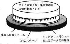
5 ( ) MEBDW Multiple Electron Beam Direct Write (J. Vac. Sci. Technol. B18(6), Nov/Dec )


6 (P.N.Minh, MEMS 04 (2004), p.430)


7

8 (Fowler-Nordheim plot)

, 43")
9 Si-MFE (Micro Field Emitter ) (SEM), 43 (2000) p.112
 p.")
")

10 (SEM), 43 (2000) p.112 (NSOM) (AFM)
 (P.H.")
 (")
11 (NSOM) (AFM) (P.H.Minh, MEMS 99) (NSOM) ( 20nm)


12 NSOM AFM NSOM AFM Optical throughput (intensity) versus aperture diameter (P. N. Minh et.al. Review of Scientific Instruments, 71,8 (2000), )
 + + + + + + + + + + + +++ - - - - - - - - - - - -")
 (K.Iwami, 4th Asia-Pasific Intern. Conf.")
13 plasmon Narrow gap (several 10 nm. It determines the resolution) Polarization Incident light plasmon Localized and highly enhanced optical near-field. Bow-tie antenna (Opposed metal triangles) (K.Iwami, 4th Asia-Pasific Intern. Conf. on Near-Field Optics (APNFO-4), Taiwan (2003 Oct.13-16) pp.55-56) NSOM
 Si 2 2")

")
14 AC turn off AFM NSOM AFM SNOM SEM Oxidation Si(100) Si 2 2 Patterning Photoresist Oxide Patterning Si Etching Super Critical Drying 20nm (X.Li et.al., MEMS 2002, Jan.22, TP41)
15 (J.Yang et.al., Appl. Phys. UHV Q Lett., 77, 2000) Laser Doppler Lens Electrode Cantilever Optical Window Phase Adjustor Filter Wave Converter Network Analyser Pulse Counter Vacuum Chamber V Computer ~ torr (UHV)

16 The mass of the CNTs bundle before storage g After hydrogen storage g The hydrogen storage capacitance 6.0 wt.% Mass resolution g 170 nm, Q (T.Ono et.al., MEMS 2001) Si w Qo RF B F B M F:Force w B: N =r B M: r: w Qo : w N : (N)MRFM [(Nuclear)Magnetic Resonace Force Microscopy]
 50nm Si 1.")
 10 4 T/m 1 1.4 10-22 N f 0 f 0 f 0 /f 0 f 0 27kHz 0.")
17 5x x10-13 Force (N) 3x x x Amplitude of Magnetic Field (mt) 50nm Si 1.5 m Fe Cantilever Coil Piezo scanner Magnet MRFM (T.Ono et.al., MEMS 2001) 10 4 T/m N f 0 f 0 f 0 /f 0 f 0 27kHz N/m Q H m Q


18 Switchable cantilever for a time-of-flight scanning force microscopy D.W.Lee, Applied Physics Letters, 84 (2004) pp

 377 /")

19 ( HORIBA Report 7 (1993) ) VO 2 ( ) 377 / 0 0 1/2 = 377 ( 117-E (1997) p.612)

 p.")
20 ( 117-E (1997) p.612) pn (M.Kimmata et.al., 2001 Intn. Conf. on Solid State Device and Materials, (2001) p.466)


21 MOS Tr


22 1

)")
23 ( ( ) MSS (2002)) ( ( ) MSS (2002))
) C 0.")


24 G : ( ) ( ( ) MSS (2002)) C 0.1K Joule/K Q 6 kev X Joule T 10 3 K) (L.Mechin et.al., Sensors & Actuators A55 (1996) p.19)
25 X (L.Mechin et.al., Sensors & Actuators A55 (1996) p.19) X ( Vol.13, No.12 (1998) p.18)
 p.18) (T.")

26 X ( Vol.13, No.12 (1998) p.18) (T.Ono, Jpn. J. Appl. Phys., 42, Part 1, No.6B, p.3867 (2003) )
 (e)")


27 (b) (c) (d) (e) PMMA Moth-Eye-Effect ( technotrans ) ( )
 ( ) ( )")
28 S.C.Terry, Ph.D. dissertation Stanford University (1975) S.C.Terry et.al, IEEE Tras. On Electron Devices, ED (1979) ( ) ( )

29 Si


30


31


, Solid-State")

32 Ion Mobility Spectrometer (R.A.Miller (Charles Stark Draper Lab.), Solid-State Sensor and Actuator Workshop, p.120 (2000))


33 IMS ESI (Electrospray ionization) (X.-Q.Wang, MEMS 99, p.523 (1999))


34 ESI (Electrospray ionization) (X.-Q.Wang, MEMS 99, p.523 (1999))


35 20mm (M.Esashi et.al., Transducers 87, )


36


37 (K.Hirata et.al., Transducers 2001, ) 20mm


38 ( )

39 ( )


40

 pp.")
41 (M.Schwarz et.al. : Sensors & Actuators, 83 (2000) pp.40-46)


42 PTCA (Percutaneous Transluminal Angioplasty)


43 (SMA)


44 (K.-T.Park, IEEE J. of Microelectromechanical Systems, 8,p.349 (1999))


45 (Y.Haga et.al. MEMS 2000, ) ( )


46 SMA


47 1mm


48 0.5mm 0.5mm (T.Mineta et.al., Transducers 2001, )


49

50 3 mm (M.Fujita et.al., Sensor symposium, (May 2002))
 -0.03 0.0 2.0x10⁻⁶ 4.0x10⁻⁶ 6.0x10⁻⁶ 8.0x10⁻⁶ 1.0x10⁻⁵ Time (sec) Intensity (V) 0.")
51 5.5x x x x x x x Intensity (V) Intensity (V) x10 6.0x x x x x x x x x x x10-5 Time (sec) x x x x x10-5 Time (sec) Intensity (V) x10 6.0x x x x x x10-6 Intensity (V) x x x x x x x x x x x x10-5 Time (sec) x x x x x10-5 Time (sec) Intensity (V) x x x x x x x10-6 Intensity (V) x x x x x x x x10 4.0x10 6.0x10 8.0x10 1.0x10 Time (sec) Intensity (V) x x x x x x x10-6 Intensity (V) x10 4.0x10 6.0x10 8.0x10 1.0x10 Time (sec) x x x x x x x x x x x x10-5 Time (sec) x x x x x10-5 Time (sec)
 p.857) Post-CMOS CMUT (Capacitive Micromachined Ultrasonic Transducer) (R.O.Guildiken, MEMS2005 p.")
52 Lower electrode (signal electrode ) 1mm Upper electrode (common electrode) Flat US transducer Convex shaped US transducer 8-elements ring-array convex shape transducer (J.J.Chen, MEMS 04 (2004) p.857) Post-CMOS CMUT (Capacitive Micromachined Ultrasonic Transducer) (R.O.Guildiken, MEMS2005 p.315)


53 CMUT (Capacitive Micromachined Ultrasonic Transducer) (R.O.Guildiken, MEMS2005 p.315) (,120-E,5 (2000) p.211)


54 CG CG MRI


55 (N.Kikuchi et.al., Transducers'03, Boston (2003 June 9-12)) 1mm
 4 (T.")
 (K.")
56 5 mm Φ 3.8 mm 1 mm PC (Cr) 4 (T.Katsumata et.al., Optical MEMS 97) (K. Totsu et.al., Transducers 03 (2003) )


57


58 125µm Si Optical fiber


59 Optical fiber USB PC B5 size Hear Optical fiber Coupler Spectrometer White light Source 100µm ( ))


60 500Hz ~ ~


61 Ion Sensitive Field Effect Transistor ( 46 ) (Supplement to the J.J.AP.,44 (1975), )


62 ISFET ISFET ph PCO 2 (Med.& Biol.Eng.& Comp.,18 (1980) p.741)

63 ISFET ph PCO 2 ISFET ph
 2 CO + 2H")

64 ISFET (NH 2 ) 2 CO + 2H 2 O + H + 2NH HCO 3


")
65 ISFET ISFET ph (R.Chida et.al., J. of Dental Research, 65 (1986) )
 ISFET (Supplement to the J.J.AP.")
66 Si 3 N 4 surface Al 2 O 3 +SiO 2 surface ph pna ISFET M.Esashi et.al. IEEE Trans. on Electron Devices ED (1979) ISFET (Supplement to the J.J.AP.,44 (1975), )

67 ISFET (S.Shoji et.al., Sensors and Actuators, 14 (1988) pp )

68 (i-stat)


69


70 (CD ) (M.J.Madou, Biomedical Microdevices, 3, 3 (2001) pp ) (CD )


71 100 l 15 7 CD (M.Esashi et.al. : Sensors and Actuators, 20,1/2 (1990), )


72 ( ) 20 mm

73 ( CHS 00 7 (2000)) (S.C.Jacobson, Solid State Sensors and Actuators Workshop, p93 (1998))

74 ( ) (K.Handique et.al., Solid State Sensor & Actuator Workshop, Hilton Head (1998))

")


75 Deep RIE QCM (Quarts Crystal Microbalance) (L, Li et.al., Proc. of the 21th Sensor Symp., Kyoto, (2004) pp.19-22)
 pp.")
76 Spherical bi-convex QCM : : (a) Planer QCM (b) Sperical Bi-convex QCM QCM QCM (L, Li et.al., Proc. of the 21th Sensor Symp., Kyoto, (2004) pp.19-22)
IC NMOS ( )
") 5. MEMS 3 : IC NMOS ( ) (T.Hoshino (Tokyo Electron Ltd.) et.al., 18 th Sensor Symposium late news, 2001) 10000 memory : Probe (pad) Count 4000 Cobra probe cards 2000 ASIC 200 LCD driver IC Epoxy-needle
5. MEMS 3 : IC NMOS ( ) (T.Hoshino (Tokyo Electron Ltd.) et.al., 18 th Sensor Symposium late news, 2001) 10000 memory : Probe (pad) Count 4000 Cobra probe cards 2000 ASIC 200 LCD driver IC Epoxy-needle
untitled
 ( ) ( ) 1 MEMS : MEMS ( +13% / ) 2 3 ISFET ph,co 2 (K.Shimada, M.Esashi, Med.& Biol.Eng.& Comp.,18 (1980) p.741) (M.Esashi T.Matsuo, Supplement to the J.J.AP.,44 (1975),339-343) 4 5 (Y.Matsumoto, S.Shoji,
) ( ) ( 34,3 (1995))
 ( ) ( 34,3 (1995))") 4. MEMS 2 : MEMS ( ) DMD (Digital Micro mirror Device) FED (Field Emission Display) ( ) ( ) RF ( ) ( ) IC RF ( ) ) ( ) ( 34,3 (1995)) (M.Murata et.al.: IEICE Trans. Electron., E84-c (2001) p.1792) ( )
4. MEMS 2 : MEMS ( ) DMD (Digital Micro mirror Device) FED (Field Emission Display) ( ) ( ) RF ( ) ( ) IC RF ( ) ) ( ) ( 34,3 (1995)) (M.Murata et.al.: IEICE Trans. Electron., E84-c (2001) p.1792) ( )
untitled
 1. 2. ( ) 3. ( ) 4. ( ) 5. ( ) 6. MEMS 20mm 400 (40 )100 A-A A 2. ( ) MEMS A (L.M.Roylance et.al., IEEE Trans. on Electron Devices, ED-26 (1979) p.1911) ( (In-Vivo Oximetry)) (J.M.Schmitt,F.G.Mihm and
( )
") MEMS 4 : ( ) ( ) Pt ITO Si (2 m) Si (0.2 m) (T.Ono et.al., J.Micromech.Microeng.,10 (2000) 445-451) DEMA (Distributed Electrostatic MicroActuator) (XY ) DEMA (Distributed Electrostatic MicroActuator)
MEMS 4 : ( ) ( ) Pt ITO Si (2 m) Si (0.2 m) (T.Ono et.al., J.Micromech.Microeng.,10 (2000) 445-451) DEMA (Distributed Electrostatic MicroActuator) (XY ) DEMA (Distributed Electrostatic MicroActuator)
) ( ) ( 34,3 (1995))
 ( ) ( 34,3 (1995))") 4. MEMS 2 : MEMS ( ) DMD (Digital Micro mirror Device) FED (Field Emission Display) ( ) ( ) RF ( ) ( ) IC RF ( ) ) ( ) ( 34,3 (1995)) (M.Murata et.al.: IEICE Trans. Electron., E84-c (2001) p.1792) ( )
4. MEMS 2 : MEMS ( ) DMD (Digital Micro mirror Device) FED (Field Emission Display) ( ) ( ) RF ( ) ( ) IC RF ( ) ) ( ) ( 34,3 (1995)) (M.Murata et.al.: IEICE Trans. Electron., E84-c (2001) p.1792) ( )
10 nm SThM Fig.1 AFM 6) AFM 7) Fig.1 AFM 0.1 N/m 100 pn 10 nn 8) SThM STM AFM RTD Resistance Temperature Device SNOM Scanning Near-field Optical Micro
 AFM 7) Fig.1 AFM 0.1 N/m 100 pn 10 nn 8) SThM STM AFM RTD Resistance Temperature Device SNOM Scanning Near-field Optical Micro") @@@@@@@@@@@@@@ @@@@@@@@@@@@@@@@@@@@@@@@@@@@@@@@@@@@@@@@@@@@@@@@@@@@@@@@@@@@@@@@@@@@@@@@@@@@@@@@@@@@@@@@@@@@@@@@@@@@@@@@@@@@@@@@@@@@@@@@@@@@@@@@@@@@@@@@@@@@@@@@@@@@@@@@@@@@@@@@@@@@@@@@@@@@@@@@@@@@@@@@@@@@@@@@@@@@@@@@@@@@@@@@
@@@@@@@@@@@@@@ @@@@@@@@@@@@@@@@@@@@@@@@@@@@@@@@@@@@@@@@@@@@@@@@@@@@@@@@@@@@@@@@@@@@@@@@@@@@@@@@@@@@@@@@@@@@@@@@@@@@@@@@@@@@@@@@@@@@@@@@@@@@@@@@@@@@@@@@@@@@@@@@@@@@@@@@@@@@@@@@@@@@@@@@@@@@@@@@@@@@@@@@@@@@@@@@@@@@@@@@@@@@@@@@
Introduction to Microfabrication
 2005 Introduction to Microfabrication 1 1.1 Microfabrication disciplines Microfabrication technologies IC industry and related industries MEMS, solar cells, flat-panel displays, optelectronics In-plane
16 (16) poly-si mJ/cm 2 ELA poly-si super cooled liquid, SCL [3] a-si poly-si [4] solid phase crystalization, SPC [5] mJ/cm 2 SPC SCL (di
![16 (16) poly-si mJ/cm 2 ELA poly-si super cooled liquid, SCL [3] a-si poly-si [4] solid phase crystalization, SPC [5] mJ/cm 2 SPC SCL (di](/thumbs/82/84964999.jpg "16 (16) poly-si mJ/cm 2 ELA poly-si super cooled liquid, SCL [3] a-si poly-si [4] solid phase crystalization, SPC [5] mJ/cm 2 SPC SCL (di") (15) 15 ELA により形成された poly-si 結晶成長様式 - グレイン形状と水素の関係 - Crystal Growth Mode of Poly-Si Prepared by ELA -Relationship between the Grain Morphology and ydrogens- Naoya KAWAMOTO (Dept. of Electrical and Electronic
(15) 15 ELA により形成された poly-si 結晶成長様式 - グレイン形状と水素の関係 - Crystal Growth Mode of Poly-Si Prepared by ELA -Relationship between the Grain Morphology and ydrogens- Naoya KAWAMOTO (Dept. of Electrical and Electronic
03_委託テーマ発表資料(その2)(p.89-p.134).pdf
(p.89-p.134).pdf") 89 MEMS 2 / 5-0 0-20 90 3 Beyond-CMOS CNT CNT CNT NEC 4 NEDO (80 NEDO 2008.05 Nature Nanotechnology NEDO (8 22 CNT CNT NEDOPJ CNT NEDO M 3 5 Nature Nanotechnology 3, 289-294 (2008) 6 9 7 8 92 9 (!!! '!!!
89 MEMS 2 / 5-0 0-20 90 3 Beyond-CMOS CNT CNT CNT NEC 4 NEDO (80 NEDO 2008.05 Nature Nanotechnology NEDO (8 22 CNT CNT NEDOPJ CNT NEDO M 3 5 Nature Nanotechnology 3, 289-294 (2008) 6 9 7 8 92 9 (!!! '!!!
スライド 1
 swk(at)ic.is.tohoku.ac.jp 2 Outline 3 ? 4 S/N CCD 5 Q Q V 6 CMOS 1 7 1 2 N 1 2 N 8 CCD: CMOS: 9 : / 10 A-D A D C A D C A D C A D C A D C A D C ADC 11 A-D ADC ADC ADC ADC ADC ADC ADC ADC ADC A-D 12 ADC
日立評論2008年1月号 : 基盤技術製品
 Infrastructure Technology / Products HIGHLIGHTS 2008 HDD 2.5 HDD3.5 HDD 1 Deskstar 7K1000 HDD Hard Disk Drive 2006 5 PC 2.5 HDD HDD 3.5 HDD1 1 2007 3Deskstar 7K1000 3.5 HDD 1149 Deskstar 7K500 2 GMR Giant
スライド 1
 CMOS : swk(at)ic.is.tohoku.ac.jp [ 2003] [Wong1999] 2 : CCD CMOS 3 : CCD Q Q V 4 : CMOS V C 5 6 CMOS light input photon shot noise α quantum efficiency dark current dark current shot noise dt time integration
Company_2801.ai
 Park Systems www.parkafm.co.jp Park Systems Enabling Nanoscale Advances ㅣ ㅣ ㅣ ㅣ ㅣ ㅣ ㅣ ㅣ ㅣ ㅣ ㅣ ㅣ ㅣ ㅣ ㅣ ㅣ ㅣ Courtesy NASA/JPL-Caltech Park Systems Enabling Nanoscale Advances 5 98 988 997 Prof. C.F. Quate
Microsoft PowerPoint - 山形大高野send ppt [互換モード]
![Microsoft PowerPoint - 山形大高野send ppt [互換モード]](/thumbs/96/127884904.jpg "Microsoft PowerPoint - 山形大高野send ppt [互換モード]") , 2012 10 SCOPE, 2012 10 2 CDMA OFDMA OFDM SCOPE, 2012 10 OFDM 0-20 Relative Optical Power [db] -40-60 10 Gbps NRZ BPSK-SSB 36dB -80-20 -10 0 10 20 Relative Frequency [GHz] SSB SSB OFDM SSB SSB OFDM OFDM
, 2012 10 SCOPE, 2012 10 2 CDMA OFDMA OFDM SCOPE, 2012 10 OFDM 0-20 Relative Optical Power [db] -40-60 10 Gbps NRZ BPSK-SSB 36dB -80-20 -10 0 10 20 Relative Frequency [GHz] SSB SSB OFDM SSB SSB OFDM OFDM
技術創造の社会的条件
 1999 10 21 21 i ... 1 1... 3 1-1. 20...3 1900 1945 3 1945 198x 4 198x 1999 5 1-2....7 1945 198x 7 HEMT 8 198x 1999 9 9 1-3....11 11 12 13 18 2 New Institutions... 21 2-1....21 22 24 26 2-2....27 28 29
J. Mass Spectrom. Soc. Jpn.: 58(5), (2010)
, (2010)") J. Mass Spectrom. Soc. Jpn. Vol. 58, No. 5, 2010 REVIEW 9 Secondary Ion Mass Spectrometry (SIMS) SIMS SIMS Fundamentals of Mass Spectrometry Secondary Ion Mass Spectrometry (SIMS), Cluster SIMS, and Electrospray
J. Mass Spectrom. Soc. Jpn. Vol. 58, No. 5, 2010 REVIEW 9 Secondary Ion Mass Spectrometry (SIMS) SIMS SIMS Fundamentals of Mass Spectrometry Secondary Ion Mass Spectrometry (SIMS), Cluster SIMS, and Electrospray
untitled
 1 1-1 p-i-n 1-1 (CIS/CIGS CdTe ) (GaAs) (,,) (, ) (,,) Si Si Si (CIS/CIGS CdTe ) (GaAs) (,,) (, ) (,,) Si Si Si Si 1-2 HITHeterojunction with Intrinsic Thin layer 30 HIT 22.3NIKKEI MICRODEVICES, May,82-86(2008)
2 ( ) PVD (Physical Vapor Deposition)
 PVD (Physical Vapor Deposition)") 2 ( ) PVD (Physical Vapor Deposition) G.Lim et.al., Robotica, 14 (1996) pp.499-506 ( ) ( Ionics, 20, 9 (1994) p.147) MEMS CVD (Chemical Vapor Deposition) CVD MacDonald et.al. MEMS 90 CVD 160-220ºC 1,1,1,5,5,5,5-
2 ( ) PVD (Physical Vapor Deposition) G.Lim et.al., Robotica, 14 (1996) pp.499-506 ( ) ( Ionics, 20, 9 (1994) p.147) MEMS CVD (Chemical Vapor Deposition) CVD MacDonald et.al. MEMS 90 CVD 160-220ºC 1,1,1,5,5,5,5-
食糧 その科学と技術 No.43( )
") 17 DNA SEM, Scanning electron microscope TEM, transmission electron microscope X NMR AFM, atomic force microscopy SPM, scanning probe microscopy 1 SPM SPM AFM SNOM NSOM, Scanning near-field optical microscope
17 DNA SEM, Scanning electron microscope TEM, transmission electron microscope X NMR AFM, atomic force microscopy SPM, scanning probe microscopy 1 SPM SPM AFM SNOM NSOM, Scanning near-field optical microscope
i
 i ii 1 6 9 12 15 16 19 19 19 21 21 22 22 23 26 32 34 35 36 3 37 5 5 4 4 5 iii 4 55 55 59 59 7 7 8 8 9 9 10 10 1 11 iv ozein Van Marum 1801 Cruiokshank Marum 1840 Schonbein 3 / atm 1 N 1892 50 1960 1970
テストコスト抑制のための技術課題-DFTとATEの観点から
 2 -at -talk -talk -drop 3 4 5 6 7 Year of Production 2003 2004 2005 2006 2007 2008 Embedded Cores Standardization of core Standard format Standard format Standard format Extension to Extension to test
日立評論 2016年5月号:収差補正器のSTEM(HD-2700),TEM(HF-3300S),1.2 MV FIRSTプログラム向け開発,そして将来への展望
,TEM(HF-3300S),1.2 MV FIRSTプログラム向け開発,そして将来への展望") 明日の科学と社会の発展に貢献する計測 分析技術 収差補正器の STEM(HD-27),TEM(HF-33S), 1.2 MV FIRST プログラム向け開発, そして将来への展望 Prof. Dr. Max. Haider Dr. Heiko Müller [ 特集監修者抄録 ] 電子顕微鏡では, 電子レンズが持つ球面収差により, 分解能向上が長らく阻まれてきた 199 年代中盤にようやく, 成功し,
明日の科学と社会の発展に貢献する計測 分析技術 収差補正器の STEM(HD-27),TEM(HF-33S), 1.2 MV FIRST プログラム向け開発, そして将来への展望 Prof. Dr. Max. Haider Dr. Heiko Müller [ 特集監修者抄録 ] 電子顕微鏡では, 電子レンズが持つ球面収差により, 分解能向上が長らく阻まれてきた 199 年代中盤にようやく, 成功し,
 1-x x µ (+) +z µ ( ) Co 2p 3d µ = µ (+) µ ( ) W. Grange et al., PRB 58, 6298 (1998). 1.0 0.5 0.0 2 1 XMCD 0-1 -2-3x10⁻³ 7.1 7.2 7.7 7.8 8.3 8.4 up E down ρ + (E) ρ (E) H, M µ f + f E F f + f f + f X L
2章.doc
 C 2 H 4 N 2 O 2 LPG LIF 13 2.1 2.1.1 2.1 2.2 115mm70mm 727cm 3 Hand Pump Injector Driver Computer Constant Volume Chamber Injector Piezo-electronic transducer Fan Spark Plug Temperature Indicator C 2 H
研究成果報告書
 10m 2m Ge Si BaF2 ZnSZnSe Sb-Ge-Sn-S IIR-SF1 1 2 Tungsten SilicideWSi WSi () IIR-SF 1 Sb-Ge-Sn-S 0.85~11μm2.710μm 253 C Al Al 220μm He-Cd laser 1 Exposure Photoresist WSi (a) 500 nm Development RIE WSi
 155 13 2 15 B97176 1 1.1. 4 1.2. 5 1.2.1. 1.2.2. 1.3. 7 2. 2.1. 9 2.2. 1 2.3. 13 2.4. 16 3. 3.1. 3.1.1. 18 3.1.2. 26 3.1.3. 33 3.2. 3.2.1. 34 3.2.2. 5 4. 4.1. 52 4.2. 53 54 55 2 1 1.1 1.2 1.3 3 4 Fig.
Siマイクロマシニングと集積化技術.PDF
 ケミカル エンジニアリング(化学工業社) 25 年 9 月号 pp.731-735. シリコンマイクロマシニングと集積化技術 佐々木実*1 金森義明*2 羽根一博*3 Minoru Sasaki, Yoshiaki Kanamori, Kazuhiro Hane 東北大学大学院工学研究科 *1 助教授 工学博士 *2 助手 工学博士 *3 教授 工学博士 1 はじめに LSI に代表される半導体産業の黎明期にフォト
Telescope aperture 1.5mφ Telescope length Fit within the H-IIA nose fairing Spatial resolution 0.1" in UV 0.16" in Vis/NIR (Diffraction limit of 1.5mφ
 , (NAOJ) (Kyoto U.) Telescope aperture 1.5mφ Telescope length Fit within the H-IIA nose fairing Spatial resolution 0.1" in UV 0.16" in Vis/NIR (Diffraction limit of 1.5mφ at 1µm ) FOV ~200" x 200" to cover
PowerPoint Presentation
 / 2008/04/04 Ferran Salleras 1 2 40Gb/s 40Gb/s PC QD PC: QD: e.g. PCQD PC/QD 3 CP-ON SP T CP-OFF PC/QD-SMZ T ~ps, 40Gb/s ~100fJ T CP-ON CP-OFF 500µm500µm Photonic Crystal SMZ K. Tajima, JJAP, 1993. Control
1章
 19 1 11 12 2 21 22 3 31 32 33 1 2 34 4 41 42 43 44 5 51 52 53 54 55 56 57 6 61 62 63 64 65 7 8 81 82 11,,,,,,,,, 12,,,,,,,,,, Table121,,,,,,2 21 Table121 Noncontact mechanism (5) ( ) (1),,,,,,,,,,,,,,,,,,,,,,,,,,,,,
Temperature Rise in a Birefringent Substrate by RF Discharge Plasma Koichi Takaki, Member, Kunioh Sayama, Student Member, Atsushi Takahashi, Student M
 Temperature Rise in a Birefringent Substrate by RF Discharge Plasma Koichi Takaki, Member, Kunioh Sayama, Student Member, Atsushi Takahashi, Student Member, Tamiya Fujiwara, Member (Iwate University),
untitled
 /Si FET /Si FET Improvement of tunnel FET performance using narrow bandgap semiconductor silicide Improvement /Si hetero-structure of tunnel FET performance source electrode using narrow bandgap semiconductor
修士論文
 SAW 14 2 M3622 i 1 1 1-1 1 1-2 2 1-3 2 2 3 2-1 3 2-2 5 2-3 7 2-3-1 7 2-3-2 2-3-3 SAW 12 3 13 3-1 13 3-2 14 4 SAW 19 4-1 19 4-2 21 4-2-1 21 4-2-2 22 4-3 24 4-4 35 5 SAW 36 5-1 Wedge 36 5-1-1 SAW 36 5-1-2
36 581/2 2012
 4 Development of Optical Ground Station System 4-1 Overview of Optical Ground Station with 1.5 m Diameter KUNIMORI Hiroo, TOYOSHMA Morio, and TAKAYAMA Yoshihisa The OICETS experiment, LEO Satellite-Ground
c c SSIS10 10 10 1998 2001 SSIS 2001 LSI 2001 MIRAI NECASKA SELETE 21 5ISSCC LSI 2004 2004SSIS PR 60 70
 Encore SSIS 10 c c SSIS10 10 10 1998 2001 SSIS 2001 LSI 2001 MIRAI NECASKA SELETE 21 5ISSCC LSI 2004 2004SSIS PR 60 70 SSIS NOSIDE PR SSIS SSIS PR 2000 5SSIS SSIS 1 2001 5 8 3 2004 SSIS 1 2 SSIS 24 SSISPR
10 IDM NEC
 No.29 1 29 SEAJ SEAJ 2 3 63 1 1 2 2002 2003 6 News 9 IEDM 11 13 15 16 17 10 IDM NEC 3 12 3 10 10 2 3 3 20 110 1985 1995 1988 912001 1 1993 95 9798 199010 90 200 2 1950 2 1950 3 1311 10 3 4 4 5 51929 3
èCò_ï\éÜ.pdf
 [Co/Ru] 20 Antiferromagnetic Exchange Coupling Energy in [Co/Ru] 20 19 1...1 1.1...1 1.2...1 1.2.1...1 1.2.2...2 1.3...2 1.4...3 1.4.1...3 1.4.2...5 1.5...5 1.5.1...5 1.5.2 SF...6 1.5.3 TAMR...6 2...8
空気の屈折率変調を光学的に検出する超指向性マイクロホン
 23 2 1M36268 2 2 4 5 6 7 8 13 15 2 21 2 23 2 2 3 32 34 38 38 54 57 62 63 1-1 ( 1) ( 2) 1-1 a ( sinθ ) 2J D ( θ ) = 1 (1-1) kaka sinθ ( 3) 1-2 1 Back face hole Amplifier Diaphragm Equiphase wave surface
COE
 COE COOL05 MD @ @ @ @ n ν x, y 2 2 International Workshop on Beam Cooling and Related Topics ( COOL05) General Topics Overview. S-LSR Report from Lab Report from Lab Electron Cooling Muon Cooling
untitled
 Vol. 1 (2005) pp. 91-103 * ( 17 1 27 ) Approach from Bioelectronics to Bio-Interface Masashi YAOITA * Our studies for approach to bio-interface were fabrication of a needle type glucose sensor for continuous
The Plasma Boundary of Magnetic Fusion Devices
 ASAKURA Nobuyuki, Japan Atomic Energy Research Institute, Naka, Ibaraki 311-0193, Japan e-mail: asakuran@fusion.naka.jaeri.go.jp The Plasma Boundary of Magnetic Fusion Devices Naka Fusion Research Establishment,
untitled
 1 / 37 5-4 6.1 1 2 / 37 1 (1) FePt AuAg (2) CdSe ZnSXY 2 O 3 X X : ZnO (3) SiO 2 (4) (5) 2 1 3 / 37 1 (1) FePt AuAg (2) CdSe ZnSXY 2 O 3 X X : ZnO (3) SiO 2 (4) (5) 3 4 / 37 1Tbits/cm 2 HD FePt FePt 110nm
MOSFET HiSIM HiSIM2 1
 MOSFET 2007 11 19 HiSIM HiSIM2 1 p/n Junction Shockley - - on-quasi-static - - - Y- HiSIM2 2 Wilson E f E c E g E v Bandgap: E g Fermi Level: E f HiSIM2 3 a Si 1s 2s 2p 3s 3p HiSIM2 4 Fermi-Dirac Distribution
B1 Ver ( ), SPICE.,,,,. * : student : jikken. [ ] ( TarouOsaka). (, ) 1 SPICE ( SPICE. *1 OrCAD
![B1 Ver ( ), SPICE.,,,,. * : student : jikken. [ ] ( TarouOsaka). (, ) 1 SPICE ( SPICE. *1 OrCAD](/thumbs/101/152175529.jpg "B1 Ver ( ), SPICE.,,,,. * : student : jikken. [ ] ( TarouOsaka). (, ) 1 SPICE ( SPICE. *1 OrCAD") B1 er. 3.05 (2019.03.27), SPICE.,,,,. * 1 1. 1. 1 1.. 2. : student : jikken. [ ] ( TarouOsaka). (, ) 1 SPICE ( SPICE. *1 OrCAD https://www.orcad.com/jp/resources/orcad-downloads.. 1 2. SPICE 1. SPICE Windows
B1 er. 3.05 (2019.03.27), SPICE.,,,,. * 1 1. 1. 1 1.. 2. : student : jikken. [ ] ( TarouOsaka). (, ) 1 SPICE ( SPICE. *1 OrCAD https://www.orcad.com/jp/resources/orcad-downloads.. 1 2. SPICE 1. SPICE Windows
Canvas-tr01(title).cv3
.cv3") Working Group DaiMaJin DaiRittaikaku Multiparticle Jiki-Bunnsekiki Samurai7 Superconducting Analyser for Multi particles from RadioIsotope Beams with 7Tm of bending power (γ,n) softgdr, GDR non resonant
Working Group DaiMaJin DaiRittaikaku Multiparticle Jiki-Bunnsekiki Samurai7 Superconducting Analyser for Multi particles from RadioIsotope Beams with 7Tm of bending power (γ,n) softgdr, GDR non resonant
42 1 Fig. 2. Li 2 B 4 O 7 crystals with 3inches and 4inches in diameter. Fig. 4. Transmission curve of Li 2 B 4 O 7 crystal. Fig. 5. Refractive index
 MEMOIRS OF SHONAN INSTITUTE OF TECHNOLOGY Vol. 42, No. 1, 2008 Li 2 B 4 O 7 (LBO) *, ** * ** ** Optical Scatterer and Crystal Growth Technology of LBO Single Crystal For Development with Optical Application
2003/3 Vol. J86 D II No.3 2.3. 4. 5. 6. 2. 1 1 Fig. 1 An exterior view of eye scanner. CCD [7] 640 480 1 CCD PC USB PC 2 334 PC USB RS-232C PC 3 2.1 2
![2003/3 Vol. J86 D II No.3 2.3. 4. 5. 6. 2. 1 1 Fig. 1 An exterior view of eye scanner. CCD [7] 640 480 1 CCD PC USB PC 2 334 PC USB RS-232C PC 3 2.1 2](/thumbs/42/22941906.jpg "2003/3 Vol. J86 D II No.3 2.3. 4. 5. 6. 2. 1 1 Fig. 1 An exterior view of eye scanner. CCD [7] 640 480 1 CCD PC USB PC 2 334 PC USB RS-232C PC 3 2.1 2") Curved Document Imaging with Eye Scanner Toshiyuki AMANO, Tsutomu ABE, Osamu NISHIKAWA, Tetsuo IYODA, and Yukio SATO 1. Shape From Shading SFS [1] [2] 3 2 Department of Electrical and Computer Engineering,
Curved Document Imaging with Eye Scanner Toshiyuki AMANO, Tsutomu ABE, Osamu NISHIKAWA, Tetsuo IYODA, and Yukio SATO 1. Shape From Shading SFS [1] [2] 3 2 Department of Electrical and Computer Engineering,
sumi.indd
 S/N S/N CCDCMOS CCD CMOS & E-mail hirofumi.sumi@jp.sony.com & E-mail Tadakuni.Narabu@jp.sony.com & E-mail Shinichiro.Saito@jp.sony.com Hirofumi SUMI, Non - Member and Tadakuni NARABU, Member and Shinichiro
untitled
 213 74 AlGaN/GaN Influence of metal material on capacitance for Schottky-gated AlGaN/GaN 1, 2, 1, 2, 2, 2, 2, 2, 2, 2, 1, 1 1 AlGaN/GaN デバイス ① GaNの優れた物性値 ② AlGaN/GaN HEMT構造 ワイドバンドギャップ半導体 (3.4eV) 絶縁破壊電界が大きい
untitled
 (a) (b) (c) (d) (e) (f) (g) (f) (a), (b) 1 He Gleiter 1) 5-25 nm 1/2 Hall-Petch 10 nm Hall-Petch 2) 3) 4) 2 mm 5000% 5) 1(e) 20 µm Pd, Zr 1(f) Fe 6) 10 nm 2 8) Al-- 1,500 MPa 9) 2 Fe 73.5 Si 13.5 B 9 Nb
IEEE HDD RAID MPI MPU/CPU GPGPU GPU cm I m cm /g I I n/ cm 2 s X n/ cm s cm g/cm
 Neutron Visual Sensing Techniques Making Good Use of Computer Science J-PARC CT CT-PET TB IEEE HDD RAID MPI MPU/CPU GPGPU GPU cm I m cm /g I I n/ cm 2 s X n/ cm s cm g/cm cm cm barn cm thn/ cm s n/ cm
Summary 3D cinemas are becoming real thanks to digital image processing technology. The most feasible and stable technology based on the binocular dis
 Summary 3D cinemas are becoming real thanks to digital image processing technology. The most feasible and stable technology based on the binocular disparity requires stereoglasses. However, there is still
Undulator.dvi
 X X 1 1 2 Free Electron Laser: FEL 2.1 2 2 3 SACLA 4 SACLA [1]-[6] [7] 1: S N λ [9] XFEL OHO 13 X [8] 2 2.1 2(a) (c) z y y (a) S N 90 λ u 4 [10, 11] Halbach (b) 2: (a) (b) (c) (c) 1 2 [11] B y = n=1 B
光学
 Si Nano-Photodiode with Surface-Plasmon Antenna Junichi FUJIKATA, Keishi OHASHI and Toru MOGAMI We studied the surface plasmon SP resonance effect on Si nano-photodiode PD characteristics for future optical
着色斜め蒸着膜の光学的性質~無機偏光膜への応用
 Anisotropy in the Optical Absorption of Metal-insulator Obliquely Deposited Thin Films The Application for an Inorganic Polarizer Motofumi Suzuki, Yasunori Taga Abstract An attempt has been made to clarify
Donald Carl J. Choi, β ( )
") :: α β γ 200612296 20 10 17 1 3 2 α 3 2.1................................... 3 2.2................................... 4 2.3....................................... 6 2.4.......................................
:: α β γ 200612296 20 10 17 1 3 2 α 3 2.1................................... 3 2.2................................... 4 2.3....................................... 6 2.4.......................................
光学
 Range Image Sensors Using Active Stereo Methods Kazunori UMEDA and Kenji TERABAYASHI Active stereo methods, which include the traditional light-section method and the talked-about Kinect sensor, are typical
DC-DC Control Circuit for Single Inductor Dual Output DC-DC Converter with Charge Pump (AKM AKM Kenji TAKAHASHI Hajime YOKOO Shunsuke MIWA Hiroyuki IW
 DC-DC Control Circuit for Single Inductor Dual Output DC-DC Converter with Charge Pump (AKM AKM Kenji TAKAHASHI Hajime YOKOO Shunsuke MIWA Hiroyuki IWASE Nobukazu TAKAI Haruo KOBAYASHI Takahiro ODAGUCHI
1
 5-3 Photonic Antennas and its Application to Radio-over-Fiber Wireless Communication Systems LI Keren, MATSUI Toshiaki, and IZUTSU Masayuki In this paper, we presented our recent works on development of
Introduction MPPC is new semiconductor photon sensor Technology is very similar to SiPM. Under development by Hamamatsu Photonics (HPK) MPPC have not
 MPPC have not") Multi Pixel Photon Counter T. Nakadaira KEK Introduction MPPC is new semiconductor photon sensor Technology is very similar to SiPM. Under development by Hamamatsu Photonics (HPK) MPPC have not been listed
Multi Pixel Photon Counter T. Nakadaira KEK Introduction MPPC is new semiconductor photon sensor Technology is very similar to SiPM. Under development by Hamamatsu Photonics (HPK) MPPC have not been listed
75 unit: mm Fig. Structure of model three-phase stacked transformer cores (a) Alternate-lap joint (b) Step-lap joint 3 4)
 Alternate-lap joint (b) Step-lap joint 3 4)") 3 * 35 (3), 7 Analysis of Local Magnetic Properties and Acoustic Noise in Three-Phase Stacked Transformer Core Model Masayoshi Ishida Kenichi Sadahiro Seiji Okabe 3.7 T 5 Hz..4 3 Synopsis: Methods of local
3 * 35 (3), 7 Analysis of Local Magnetic Properties and Acoustic Noise in Three-Phase Stacked Transformer Core Model Masayoshi Ishida Kenichi Sadahiro Seiji Okabe 3.7 T 5 Hz..4 3 Synopsis: Methods of local

光産業の将来ビジョン―ボーダレス化の中での進化と展開―(1BIZYON)
") SiRi Group 2008 2012 SRI PC19981000 3 1000 2010 100 10 2003 2010 20102000 30 2 5 10 30 2 5 10 10% 1970 1980 1990 30 2 5 10 30 2 5 10 10% 1970 1980 1990 18 2 2~3 3:3:3 18 2 2~3 3:3:3
SiRi Group 2008 2012 SRI PC19981000 3 1000 2010 100 10 2003 2010 20102000 30 2 5 10 30 2 5 10 10% 1970 1980 1990 30 2 5 10 30 2 5 10 10% 1970 1980 1990 18 2 2~3 3:3:3 18 2 2~3 3:3:3
PowerPoint プレゼンテーション
 Drain Voltage (mv) 4 2 0-2 -4 0.0 0.2 0.4 0.6 0.8 1.0 Gate Voltage (V) Vds [V] 0.2 0.1 0.0-0.1-0.2-10 -8-6 -4-2 0 Vgs [V] 10 1000 1000 1000 1000 (LSI) Fe Catalyst Fe Catalyst Carbon nanotube 1~2 nm
untitled
 2013 74 Tokyo Institute of Technology AlGaN/GaN C Annealing me Dependent Contact Resistance of C Electrodes on AlGaN/GaN, Tokyo Tech.FRC, Tokyo Tech. IGSSE, Toshiba, Y. Matsukawa, M. Okamoto, K. Kakushima,
研究室ガイダンス(H28)福山研.pdf
福山研.pdf") 1 2 3 4 5 4 He M. Roger et al., JLTP 112, 45 (1998) A.F. Andreev and I.M. Lifshitz, Sov. Phys. JETP 29, 1107 (1969) Born in 2004 (hcp 4 He) E. Kim and M.H.W. Chan, Nature 427, 225 (2004); Science 305,
1 2 3 4 5 4 He M. Roger et al., JLTP 112, 45 (1998) A.F. Andreev and I.M. Lifshitz, Sov. Phys. JETP 29, 1107 (1969) Born in 2004 (hcp 4 He) E. Kim and M.H.W. Chan, Nature 427, 225 (2004); Science 305,
main.dvi
 MICE Sci-Fi 2 15 3 7 1 1 5 1.1 MICE(Muon Ionization Cooling Experiment)............. 5 1.1.1........................... 5 1.1.2............................... 7 1.1.3 MICE.......................... 10
untitled
 ITRS2005 DFM STRJ : () 1 ITRS STRJ ITRS2005DFM STRJ DFM ITRS: International Technology Roadmap for Semiconductors STRJ: Semiconductor Technology Roadmap committee of Japan 2 ITRS STRJ 1990 1998 2000 2005
X線分析の進歩36 別刷
 X X X-Ray Fluorescence Analysis on Environmental Standard Reference Materials with a Dry Battery X-Ray Generator Hideshi ISHII, Hiroya MIYAUCHI, Tadashi HIOKI and Jun KAWAI Copyright The Discussion Group
 Laser Ablation Dynamics of Amorphous Film of a Cu-Phthalocyanine Derivative Masahiro HOSODA*,**, Hiroshi FURUTANI*,**. Hiroshi FUKUMURA*,** Hiroshi MASUHARA*, Masanobu NISHII*** Nobuyuki ICHINOSE**,***,
 ArF, KrF,, CO 2 ) X MFE ITER IFE ns, MJ/ ns, MJ/ ms, MJ/ ELM JT60-SA, ITER, DEMO [µm] W 65kV 2.3A [ ] Simple estimation of the threshold thermal load on divertor surface with ELM For Carbon Divertor Case
PALL NEWS vol.126 November 2017
 PALL NEWS November 2017 Vol.126 PALL NEWS vol.126 November 2017 NEW =2000 9660 41.4 MPa 24 MPa NFPA T2.06.01 R2-2001 CAT C/90/* (1x10 6 0-28 MPa 1x10 6 29 120 C 60 C 450 Pa 340 Pa 1 MPa JIS B 8356-3/ISO
Λ (Λ ) Λ (Ge) Hyperball γ ΛN J-PARC Λ dead time J-PARC flash ADC 1 dead time ( ) 1 µsec 3
 Λ (Ge) Hyperball γ ΛN J-PARC Λ dead time J-PARC flash ADC 1 dead time ( ) 1 µsec 3") 19 Λ (Λ ) Λ (Ge) Hyperball γ ΛN J-PARC Λ dead time J-PARC flash ADC 1 dead time ( ) 1 µsec 3 1 1 1.1 γ ΛN................. 1 1.2 KEK J-PARC................................ 2 1.2.1 J-PARC....................................
19 Λ (Λ ) Λ (Ge) Hyperball γ ΛN J-PARC Λ dead time J-PARC flash ADC 1 dead time ( ) 1 µsec 3 1 1 1.1 γ ΛN................. 1 1.2 KEK J-PARC................................ 2 1.2.1 J-PARC....................................
MOSFET 6-2 CMOS 6-2 TTL Transistor Transistor Logic ECL Emitter Coupled Logic I2L Integrated
 1 -- 7 6 2011 11 1 6-1 MOSFET 6-2 CMOS 6-2 TTL Transistor Transistor Logic ECL Emitter Coupled Logic I2L Integrated Injection Logic 6-3 CMOS CMOS NAND NOR CMOS 6-4 6-5 6-1 6-2 CMOS 6-3 6-4 6-5 c 2011 1/(33)
"Moir6 Patterns on Video Pictures Taken by Solid State Image Sensors" by Okio Yoshida and Akito Iwamoto (Toshiba Research and Development Center, Tosh
 "Moir6 Patterns on Video Pictures Taken by Solid State Image Sensors" by Okio Yoshida and Akito Iwamoto (Toshiba Research and Development Center, Toshiba Corporation, Kawasaki) Reproduced resolution chart
あらゆる情報検出から赤外線データ通信まで 幅広い用途に使える 超小型 & 高感度 光センサー Ultra-compact, high-sensitivity optical sensors for various app ranging from information detection to i
 あらゆる情報検出から赤外線データ通信まで 幅広い用途に使える 超小型 & 高感度 光センサー Ultra-compact, high-sensitivity optical sensors for various app ranging from information detection to infrared data communicati lications on CITISENSOR( 当社商標
15H02248 研究成果報告書
 70Gbps ICT 100Tbps LAN 100Gbps 10Gbps 40Gbps TU Berlin 25Gbps 60Gbps (IBM) (APL 2013, APEX 2014) 10 m (Optics Express 2014) 100Gbps 3 VCSEL 4 7 図 10 変調器集積面発光レーザ 8 NRZ 48Gbps 11 図 12 製作した変調器集積 VCSEL の近視野像
mthesis.dvi
 Study of multiple electron transfer processes to Highly charged ions with microcapillary targets : 96941 2001/01/19 1 5 1.1... 5 1.2... 6 1.2.1... 6 1.2.2 Classical over barrier(cob)... 7 1.2.3... 8 1.3...
, [g/cm 3 ] [m/s] 1 6 [kg m 2 s 1 ] ,58 1, ,56 1, , ,58 1,
![, [g/cm 3 ] [m/s] 1 6 [kg m 2 s 1 ] ,58 1, ,56 1, , ,58 1,](/thumbs/70/63326930.jpg ", [g/cm 3 ] [m/s] 1 6 [kg m 2 s 1 ] ,58 1, ,56 1, , ,58 1,") 264 72 5 216 pp. 264 272 * 43.3. k, Yj; 43.38.Hz 1. 2. 2.1 1 4.8 1 2 [kg m 2 s 1 ] 1.2 1 3 [g/cm 3 ] 34 [m/s] 1.48 1 6 [kg m 2 s 1 ] 1 [g/cm 3 ] 1,48 [m/s] 1, 1 4 1 2,5 1 Tutorial on the underwater or
264 72 5 216 pp. 264 272 * 43.3. k, Yj; 43.38.Hz 1. 2. 2.1 1 4.8 1 2 [kg m 2 s 1 ] 1.2 1 3 [g/cm 3 ] 34 [m/s] 1.48 1 6 [kg m 2 s 1 ] 1 [g/cm 3 ] 1,48 [m/s] 1, 1 4 1 2,5 1 Tutorial on the underwater or
5b_08.dvi
 , Circularly Polarized Patch Antennas Combining Different Shaped Linealy Polarized Elements Takanori NORO,, Yasuhiro KAZAMA, Masaharu TAKAHASHI, and Koichi ITO 1. GPS LAN 10% [1] Graduate School of Science
( ) : 1997
 : 1997") ( ) 2008 2 17 : 1997 CMOS FET AD-DA All Rights Reserved (c) Yoichi OKABE 2000-present. [ HTML ] [ PDF ] [ ] [ Web ] [ ] [ HTML ] [ PDF ] 1 1 4 1.1..................................... 4 1.2..................................
( ) 2008 2 17 : 1997 CMOS FET AD-DA All Rights Reserved (c) Yoichi OKABE 2000-present. [ HTML ] [ PDF ] [ ] [ Web ] [ ] [ HTML ] [ PDF ] 1 1 4 1.1..................................... 4 1.2..................................
J-PARC E15 K K-pp Missing mass Invariant mass K - 3 He Formation K - pp cluster neutron Mode to decay charged particles p Λ π - Decay p Decay E15 dete
 J-PARC E15 (TGEM-TPC) TGEM M1 ( ) J-PARC E15 TPC TGEM TGEM J-PARC E15 K K-pp Missing mass Invariant mass K - 3 He Formation K - pp cluster neutron Mode to decay charged particles p Λ π - Decay p Decay
技術調査レポート(セット版)0318
0318") 1 MEMS MEMS(Micro Electro Mechanical Systems) MEMS MEMS 1990 MEMS MEMS 2 MEMS MEMS MEMS mm ( ) MEMS MST 1mm 1m Ball Semiconductor Inc. IC [2] IC [2] Si 3 MEMS 2.1 MEMS DNA MEMS 80 MEMS ABS 2.0mm 15mm 4
1 MEMS MEMS(Micro Electro Mechanical Systems) MEMS MEMS 1990 MEMS MEMS 2 MEMS MEMS MEMS mm ( ) MEMS MST 1mm 1m Ball Semiconductor Inc. IC [2] IC [2] Si 3 MEMS 2.1 MEMS DNA MEMS 80 MEMS ABS 2.0mm 15mm 4
1 Visible spectroscopy for student Spectrometer and optical spectrum phys/ishikawa/class/index.html
 1 Visible spectroscopy for student Spectrometer and optical spectrum http://www.sci.u-hyogo.ac.jp/material/photo phys/ishikawa/class/index.html 1 2 2 2 2.1................................................
untitled
 2006.2.27 Fantastic Voyage 1966 1 2006.2.27 Fantastic Voyage 2006.2.27 2 2006.2.27 How Small is Micro & Nano? 1mm 10µm 2nm 1m DNA 10 2 10 10 0 10-1 10-2 10-3 10-4 10-5 10-6 10-7 10-8 10-9 10-10 (m) Macroscopic
Vol. 21, No. 2 (2014) W 3 mm SUS304 Ni 650 HV 810 HV Ni Ni Table1 Ni Ni μm SUS mm w 50 mm l 3 mm t 2.2 Fig. 1 XY Fig. 3 Sch
 W 3 mm SUS304 Ni 650 HV 810 HV Ni Ni Table1 Ni Ni μm SUS mm w 50 mm l 3 mm t 2.2 Fig. 1 XY Fig. 3 Sch") 110 : 565-0871 2-1 567-0871 11-1 660-0811 1-9 - 1 tanigawa@jwri.osaka - u.ac.jp Influence of Laser Beam Profile on Cladding Layer TANIGAWA Daichi, ABE Nobuyuki, TSUKAMOTO Masahiro, HAYASHI Yoshihiko, YAMAZAKI
110 : 565-0871 2-1 567-0871 11-1 660-0811 1-9 - 1 tanigawa@jwri.osaka - u.ac.jp Influence of Laser Beam Profile on Cladding Layer TANIGAWA Daichi, ABE Nobuyuki, TSUKAMOTO Masahiro, HAYASHI Yoshihiko, YAMAZAKI
X線分析の進歩45
 Advances in X-Ray Chemical Analysis, Japan, 45 (2014) ISSN 0911-7806 NaCl Color Center in NaCl Takuya TSUJI, Hiroyuki IWASAKI and Jun KAWAI NaCl Color Center in NaCl Takuya TSUJI, Hiroyuki IWASAKI and
Fig. ph Si-O-Na H O Si- Na OH Si-O-Si OH Si-O Si-OH Si-O-Si Si-O Si-O Si-OH Si-OH Si-O-Si H O 6
 NMR ESR NMR 5 Fig. ph Si-O-Na H O Si- Na OH Si-O-Si OH Si-O Si-OH Si-O-Si Si-O Si-O Si-OH Si-OH Si-O-Si H O 6 Fig. (a) Na O-B -Si Na O-B Si Fig. (b) Na O-CaO-SiO Na O-CaO-B -Si. Na O-. CaO-. Si -. Al O
Terahertz Color Scanner Takeshi YASUI Terahertz THz spectroscopic imaging is an interesting new tool for nondestructive testing, security screening, b
 Terahertz Color Scanner Takeshi YASUI Terahertz THz spectroscopic imaging is an interesting new tool for nondestructive testing, security screening, biological imaging, and other applications because of
無電解めっきとレーザー照射による有機樹脂板上へのCuマイクロパターン形成
 Title 無電解めっきとレーザー照射による有機樹脂板上への Cu マイクロパターン形成 Author(s) 菊地, 竜也 ; 和智, 悠太 ; 坂入, 正敏 ; 高橋, 英明 ; 飯野, 潔 ; 片山, 直樹 Citation 表面技術, 59(8): 555-561 Issue Date 2008-08 Doc URL http://hdl.handle.net/2115/36647 Type
PowerPoint プレゼンテーション
 2004 SPring-8 2004/6/21 CMOS 2004 2007 2010 2013 nm 90 65 45 32 (nm) 1.2 0.9 0.7 0.6 High-performance Logic Technology Requirements (ITRS 2003) 10 Photoelectron Intensity (arb.units) CTR a-sio2 0.1 HfO
untitled
 TOKUSHIMA PREFECTURAL INDUSTRIAL TECHNOLOGY CENTER 1 1 1 2 3 4 2 6 7 2 9 7 1 8 9 9 7 1 8 5 1 6 4 4 5 42 7 5 3 10 7 4 3 32 15 73 40 208 236 55 120 747 96 233 1,107 1,133 1,282 712 875 5,438 11 1,889 817
OHO.dvi
 1 Coil D-shaped electrodes ( [1] ) Vacuum chamber Ion source Oscillator 1.1 m e v B F = evb (1) r m v2 = evb r v = erb (2) m r T = 2πr v = 2πm (3) eb v
Microsoft PowerPoint - TMTinst_ _summerschool_akiyama
 1 2 3 4 5 6 7 8 9 10 590nm 2200nm 0 1.739 1.713 5 1.708 1.682 10 1.678 1.652 0-10 0.061061 0.061061 11 12 13 14 15 16 17 18 19 20 21 22 23 24 25 26 27 28 29 1.0 x1.0 0.5 x0.5 0.2 x0.2 0.1 x0.1 bg/30ms
untitled
 2008-11/13 12 4 12 5 401 501 702 401 501 A-1 9:00-10:30 B-1 9:15-10:30 C-1 9:00-10:30 A-5 9:00-10:30 B-5 9:15-10:30 A A-2 10:45-12:15 B-2 10:45-12:15 C-2 10:45-12:15 A-6 10:45-12:15 B-6 10:45-12:15 A B
Vol. 19, No. 3 (2012) 207 Fig. 2 Procedures for minute wiring onto polyimide substrate. Fig. 3 Ink - jet printing apparatus as part of laser sintering
 207 Fig. 2 Procedures for minute wiring onto polyimide substrate. Fig. 3 Ink - jet printing apparatus as part of laser sintering") 206 : 316-8511 4-12 - 1 Laser Sintering Characteristics of Silver Nanoparticle Paste for Electronics Packaging YAMASAKI Kazuhiko, MAEKAWA Katsuhiro (Received January 10, 2012) Ibaraki University, Faculty
206 : 316-8511 4-12 - 1 Laser Sintering Characteristics of Silver Nanoparticle Paste for Electronics Packaging YAMASAKI Kazuhiko, MAEKAWA Katsuhiro (Received January 10, 2012) Ibaraki University, Faculty
UWB a) Accuracy of Relative Distance Measurement with Ultra Wideband System Yuichiro SHIMIZU a) and Yukitoshi SANADA (Ultra Wideband; UWB) UWB GHz DLL
 Accuracy of Relative Distance Measurement with Ultra Wideband System Yuichiro SHIMIZU a) and Yukitoshi SANADA (Ultra Wideband; UWB) UWB GHz DLL") UWB a) Accuracy of Relative Distance Measurement with Ultra Wideband System Yuichiro SHIMIZU a) and Yukitoshi SANADA (Ultra Wideband; UWB) UWB GHz DLL UWB (DLL) UWB DLL 1. UWB FCC (Federal Communications
UWB a) Accuracy of Relative Distance Measurement with Ultra Wideband System Yuichiro SHIMIZU a) and Yukitoshi SANADA (Ultra Wideband; UWB) UWB GHz DLL UWB (DLL) UWB DLL 1. UWB FCC (Federal Communications